V2S200D Digital Vibration Sensor Reference Schematic Design
The V2S200D is a high-bandwidth, digital vibration sensor designed primarily for voice pickup and mechanical vibration sensing. Utilizing advanced MEMS (Micro-Electro-Mechanical Systems) technology, this Voice Pickup Unit (VPU) captures acoustic vibrations through physical contact—often referred to as bone conduction—while remaining largely immune to ambient airborne noise. This unique characteristic makes it an essential component for high-fidelity communication in loud environments, specifically in True Wireless Stereo (TWS) earbuds, smart eyewear, and advanced industrial monitoring systems.
Overview of the V2S200D
Operating on a Pulse Density Modulation (PDM) interface, the V2S200D provides a direct digital output that simplifies the signal chain by eliminating the need for an external analog-to-digital converter (ADC). Its high Signal-to-Noise Ratio (SNR) and wide frequency response allow it to capture the subtle nuances of human speech through a user’s cranium or the mechanical signatures of precision machinery.
| Technical Specification | Value |
| Supply Voltage (VDD) | 1.6V to 3.6V |
| Interface | Digital PDM (Pulse Density Modulation) |
| Current Consumption | 650 uA (typical) |
| Signal-to-Noise Ratio | High (optimized for voice) |
| Low Power Mode | Supported via clock frequency scaling |
| Sensitivity | Optimized for vibration conduction |
| Package Type | LGA (Land Grid Array) |
| Roll-off Frequency | Optimized for voice bandwidth |
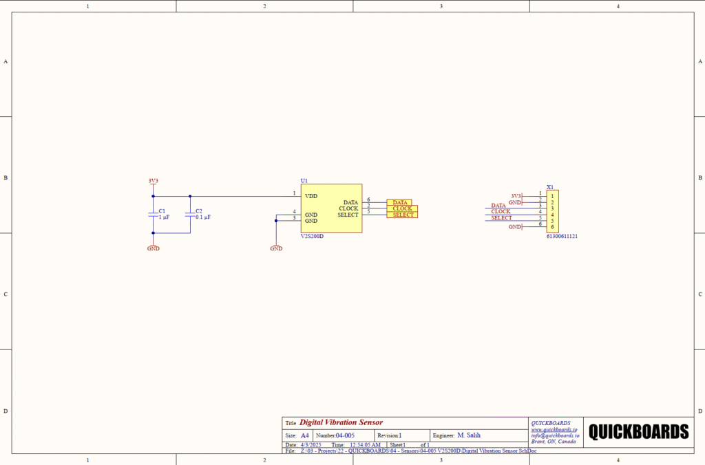
Pin Configuration and Function Mapping
The V2S200D utilizes a streamlined pinout to facilitate high-speed digital communication while maintaining a compact footprint suitable for ear-worn devices.
| Pin Number | Primary Function | Secondary / Peripheral Functions |
| 1 | VDD | Power Supply Input |
| 2 | CLOCK | PDM Clock Input |
| 3 | GND | Ground Reference |
| 4 | GND | Ground Reference |
| 5 | SELECT | Left/Right Channel Selection |
| 6 | DATA | PDM Data Output |
Functional Block Analysis & Design Decisions
Power and Decoupling Block
The power distribution for the V2S200D is supported by a dual-capacitor decoupling network consisting of C1 (1 uF) and C2 (0.1 uF). Mixed-signal MEMS devices are sensitive to supply noise, which can manifest as audible artifacts or “floor noise” in the digital output. The 0.1 uF ceramic capacitor is selected for its low equivalent series inductance (ESL) to suppress high-frequency noise generated by the internal digital modulator. The 1 uF capacitor serves as a localized bulk reservoir to stabilize the internal regulator during high-activity states. These capacitors must be placed as close as possible to Pin 1 (VDD) to minimize parasitic trace inductance.
Digital Interface and Signal Path
The digital core of the V2S200D communicates via a PDM interface, requiring a host-provided clock on Pin 2 and outputting a bitstream on Pin 6. The SELECT pin (Pin 5) is a critical configuration node; by tying this pin to VDD or GND, the designer defines whether the data is clocked on the rising or falling edge of the CLK signal. This allows two V2S200D sensors to share a single data line for stereo or array applications. In this reference design, the SELECT, CLOCK, and DATA lines are routed to the X1 header for direct integration with a host microcontroller or DSP.
Grounding and Trace Logic
Pins 3 and 4 serve as the primary ground reference for the internal analog sensing element and the digital logic. These pins must be tied to a solid ground plane to prevent ground bounce, which is a common source of jitter in high-speed PDM interfaces. The trace for the DATA line should be kept as short as possible and away from high-speed switching rails to prevent capacitive coupling and electromagnetic interference from corrupting the bitstream.
Implementation Insights
A primary engineering consideration for the V2S200D is mechanical coupling. Unlike traditional microphones, the V2S200D must have a direct mechanical path to the vibration source. In TWS applications, the sensor should be placed so that the chassis of the earbud makes firm contact with the user’s ear canal or bone structure. Any air gaps or loose mounting will severely attenuate the signal and degrade the SNR.
Another consideration involves the PDM clock frequency. The host processor must provide a stable clock within the sensor’s specified range (typically 1 MHz to 3 MHz). Deviations in clock stability can lead to phase noise in the reconstructed audio signal. It is recommended to use a high-precision oscillator or a dedicated peripheral clock from a DSP to drive the CLK pin.
Finally, while the LGA package is designed for space efficiency, it is sensitive to thermal stress during the soldering process. Designers should adhere to the manufacturer’s recommended reflow profile to prevent damage to the internal MEMS membrane, which could lead to sensitivity shifts or total device failure.
Applications
- TWS Earbuds: Bone conduction pickup for clear voice calls in extremely noisy or windy outdoor environments.
- Smart Eyewear and VR Headsets: Captures speech through the temple or forehead, allowing for voice commands without bulky boom microphones.
- Industrial Vibration Monitoring: Detects high-frequency mechanical signatures in rotating equipment for predictive maintenance.
- Secure Communications: Vibration-based pickup prevents “over-the-air” eavesdropping by ignoring airborne acoustic waves.
integrating the V2S200D into your design
The V2S200D modular block provides a validated hardware foundation for high-performance vibration and voice sensing. By utilizing a pre-tested decoupling strategy and a standardized PDM interface, this design significantly reduces the R&D time required to implement bone-conduction technology. This building block ensures that the sensitive MEMS core is correctly powered and interfaced, allowing engineering teams to focus on the high-level digital signal processing and mechanical housing design.
Skip the tedious research and manual entry. Download the production-ready schematic block for the V2S200D directly from the Quickboards Library.