LTC1661CMS 10bit Digital to Analog Reference Schematic Design
The LTC1661CMS is a micropower, dual 10-bit digital-to-analog converter (DAC) designed for applications where board space and power consumption are primary constraints. It integrates two complete, rail-to-rail voltage output DACs into a single 8-pin MSOP package. This IC is particularly well-suited for digital calibration, offset/gain adjustment, and industrial control systems. Its high-impedance reference input and low-power operation make it an industry standard for battery-powered or remote instrumentation where high accuracy and minimal thermal signature are required.
Overview of the LTC1661CMS
The device utilizes a 3-wire SPI-compatible interface to load data into two internal 10-bit shift registers. The output buffers provide excellent drive capability, allowing the analog outputs to swing from ground to the reference voltage. In this specific reference design, the DAC is paired with a dedicated low-dropout (LDO) regulator to provide a stable, precision reference voltage, ensuring that the analog output remains independent of fluctuations on the main power rail.
| Feature | Specification |
| Resolution | 10-bit |
| Number of Channels | 2 |
| Supply Voltage Range | 2.7V to 5.5V |
| Typical Supply Current | 60uA per DAC |
| Interface Type | 3-wire SPI |
| Differential Non-Linearity (DNL) | +/- 0.75 LSB (Max) |
| Settlement Time | 30us |
| Package Type | 8-pin MSOP |
Pin Configuration and Function Mapping
The LTC1661CMS utilizes an 8-pin configuration that balances high-density packaging with all necessary digital control and analog output signals.
| Pin Number | Primary Function | Secondary / Peripheral Functions |
| 1 | CS/LD | Chip Select / Load Control Input |
| 2 | SCK | Serial Clock Input |
| 3 | DIN | Serial Data Input |
| 4 | REF | Reference Voltage Input |
| 5 | VOUTB | Analog Output Channel B |
| 6 | VCC | Positive Power Supply Input |
| 7 | GND | System Ground |
| 8 | VOUTA | Analog Output Channel A |
Functional Block Analysis & Design Decisions
Power Decoupling Strategy
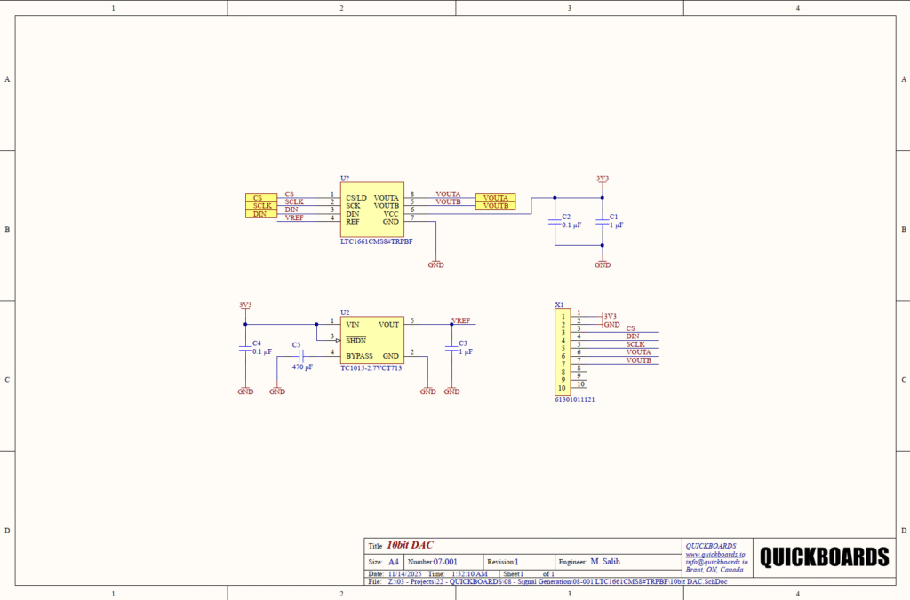
The design employs a tiered decoupling strategy for the VCC rail (Pin 6). A 1uF ceramic capacitor (C1) is paired with a 0.1uF ceramic capacitor (C2). The 0.1uF capacitor is chosen for its low equivalent series inductance (ESL), making it highly effective at filtering out high-frequency switching noise generated by the SPI digital interface. The 1uF capacitor provides bulk storage to handle lower-frequency current transients. Ceramic X7R dielectrics are specified for these components due to their high capacitance stability over voltage and temperature ranges compared to Y5V or electrolytic alternatives. These capacitors must be placed as close as possible to Pin 6 to minimize parasitic trace inductance.
Precision Voltage Reference (VREF)
A critical design choice in this block is the implementation of U2, the TC1015-2.7V LDO. While the LTC1661 can use VCC as a reference, doing so makes the analog output susceptible to power supply noise. By using a dedicated 2.7V regulator to drive the REF input (Pin 4), we establish an absolute voltage reference that is isolated from the 3.3V supply rail. The LDO output is stabilized by C3 (1uF), while C5 (470pF) is connected to the bypass pin of the TC1015 to minimize internal noise and improve the Power Supply Rejection Ratio (PSRR). This ensures the DAC maintains its 10-bit linearity even in electrically noisy environments.
Digital Interface and Connectivity
The digital control signals (CS, SCK, DIN) and analog outputs (VOUTA, VOUTB) are routed to a 10-pin header (X1). The layout for the SPI signals should maintain short, direct traces to prevent signal reflection and crosstalk. The 3.3V supply and ground are also provided on this header, allowing the module to act as a self-contained signal generation sub-system. The use of a standard header facilitates rapid prototyping and integration into larger modular backplanes.
Implementation Insights
When integrating the LTC1661CMS, pay close attention to the loading of the analog outputs. While the internal buffers are robust, driving high-capacitance loads (typically over 1000pF) may cause instability or ringing in the output voltage. If the DAC is required to drive long cables or highly capacitive inputs, an external op-amp buffer or a small series isolation resistor should be considered to maintain phase margin.
The reference input (REF) is high impedance, but it is not completely static. During a conversion cycle, internal switching can draw small amounts of charge from the reference. The placement of C3 (1uF) near Pin 4 is vital to provide a low-impedance reservoir, preventing “reference sag” which would otherwise manifest as non-linearity in the digital-to-analog conversion.
Applications
- Industrial Process Control: Precise control of 4-20mA loops or valve actuators through digital-to-analog conversion.
- Digital Calibration: Automating the calibration of gain and offset in sensitive analog front-ends.
- Battery-Powered Instruments: Low-power operation extends the operational life of handheld diagnostic tools.
- Remote Industrial Sensors: Provides local analog control signals in remote installations with limited power budgets.
Integrating the LTC1661CMS into your design
This modular schematic block provides a pre-validated hardware foundation for dual-channel analog signal generation. By utilizing a dedicated precision reference and optimized decoupling, this design eliminates the common errors associated with reference noise and supply instability. The compact footprint and standardized pin mapping allow you to drop this 10-bit DAC stage directly into your project, significantly reducing R&D time and ensuring predictable analog performance.
Skip the tedious research and manual entry. Download the production-ready schematic block for the LTC1661CMS directly from the Quickboards Library.