ADS1263IPWR 32bit Analog to Digital Converter Reference Schematic Design
The ADS1263IPWR is a high-precision, 32-bit Delta-Sigma Analog-to-Digital Converter (ADC) designed for the most demanding measurement applications. Featuring ultra-low noise, integrated Programmable Gain Amplifiers (PGA), and a high-accuracy internal reference, this IC is the gold standard for digitizing minute analog signals with extreme fidelity. It is typically employed in precision weight scales, high-resolution temperature transmitters (RTD/Thermocouple), and multi-channel industrial process control systems where the difference between a successful measurement and background noise is measured in nanovolts.
Overview of the ADS1263IPWR
As a Delta-Sigma converter, the ADS1263IPWR utilizes oversampling and noise-shaping to achieve an effectively higher resolution than standard SAR converters. Its architecture is specifically optimized for DC and low-frequency signals. With integrated sensors for system monitoring and a secondary 24-bit auxiliary ADC, it provides a comprehensive diagnostic and measurement ecosystem on a single chip.
| Feature | Specification |
| Resolution | 32-bit |
| Maximum Sample Rate | 38.4 kSPS |
| Integrated PGA Gain | 1 to 128 V/V |
| Low Noise | 7 nVrms at 2.5 SPS (Gain = 128) |
| Reference Drift | 2 ppm/degree Celsius |
| Power Supply | 2.7V to 5.25V (AVDD), 2.7V to 3.6V (DVDD) |
| Input Channels | 10 (Analog Inputs AIN0-AIN9) |
| Interface | SPI-Compatible with CRC |
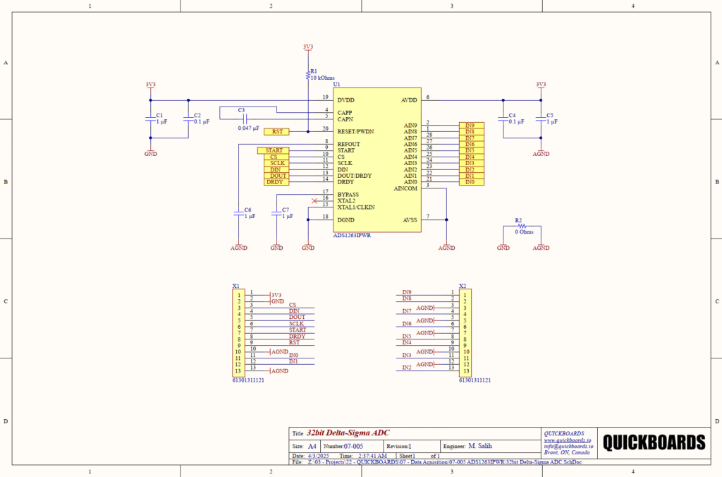
Pin Configuration and Function Mapping
The 28-pin TSSOP package provides a highly organized split between analog and digital domains, which is essential for maintaining signal integrity at 32-bit resolution.
| Pin Number | Primary Function | Secondary / Peripheral Functions |
| 6 | AVDD | Analog Power Supply |
| 19 | DVDD | Digital Power Supply |
| 7 | AVSS | Analog Ground Reference |
| 18 | DGND | Digital Ground Reference |
| 4, 5 | CAPP / CAPN | PGA Output Filter Connection |
| 20 | RESET/PWDN | Device Reset and Power-Down (Active Low) |
| 8 | REFOUT | Internal Reference Voltage Output |
| 17 | BYPASS | Internal LDO Bypass / Filter |
| 9-14 | START, CS, SCLK, DIN, DOUT/DRDY, DRDY | SPI Interface and Control Logic |
| 21-28, 1, 2 | AIN0 – AIN9 | Analog Input Channels 0 to 9 |
Functional Block Analysis & Design Decisions
Power and Decoupling Strategy
In 32-bit measurement systems, the power distribution network is a common source of measurement instability. This design utilizes a split-rail architecture, separating the Analog Supply (AVDD) from the Digital Supply (DVDD), even though both are powered by the 3.3V (3V3) rail in this configuration. Each supply pin is supported by a parallel combination of a 1uF (C1, C5) and a 0.1uF (C2, C4) ceramic capacitor. The 0.1uF capacitors are high-frequency ceramic types selected for their low equivalent series inductance (ESL) to filter logic switching noise, while the 1uF capacitors provide localized energy storage for lower-frequency transients. Placement is critical; these must be located immediately adjacent to the IC supply pins to minimize parasitic trace inductance.
Internal PGA Filtering (CAPP/CAPN)
The pins CAPP (Pin 4) and CAPN (Pin 5) allow access to the output of the integrated Programmable Gain Amplifier. A 0.047uF ceramic capacitor (C3) is placed across these pins to act as a low-pass filter for the modulator. This capacitor is essential for attenuating high-frequency noise and glitches from the modulator switching, preventing them from aliasing back into the measurement passband. A high-quality C0G or NP0 dielectric is recommended for this capacitor to ensure thermal stability and minimize voltage-coefficient-induced non-linearity.
Reference and Internal LDO Stability
The ADS1263 requires stable voltage nodes for its internal operations. REFOUT (Pin 8) provides the internal reference voltage, which is stabilized by a 1uF ceramic capacitor (C6). Similarly, the BYPASS pin (Pin 17), which is connected to the internal digital LDO, is filtered by a 1uF capacitor (C7). These capacitors are referenced to Analog Ground (AGND) to ensure the reference and internal logic remain quiet relative to the analog inputs.
Mixed-Signal Grounding (Net-Tie)
Achieving a 32-bit noise floor requires meticulous grounding. This schematic employs a “star ground” strategy where the Digital Ground (DGND) and Analog Ground (AGND) are isolated across the PCB and tied together at a single point via R2, a 0 Ohm resistor. This “net-tie” ensures that high-speed return currents from the SPI bus and digital logic do not “pollute” the analog ground plane, which could introduce significant common-mode noise into the sensitive front-end sampling circuitry.
Logic Control and Reset
The RESET/PWDN pin (Pin 20) is pulled high to the 3.3V rail through a 10kOhm resistor (R1). This defines a default “active” state, ensuring the IC does not enter a power-down or reset state due to environmental noise. This allows a host microcontroller to actively pull the line low for a hard reset if required, while maintaining a robust default operating state.
Implementation Insights
When integrating the ADS1263IPWR, the PCB layout must account for thermal EMF. At 32-bit resolution, even slight temperature gradients across dissimilar metal junctions (such as solder joints) can create microvolt-level offsets. Keeping the analog front-end layout symmetrical and away from heat-generating components (like power regulators) is essential for maintaining DC accuracy.
Another critical consideration is the settling time of the digital filter. Delta-Sigma ADCs utilize complex digital sinc filters; when a step change occurs at the input (or when switching multiplexer channels), the filter requires a finite number of conversion cycles to provide a fully settled result. Firmware must be architected to ignore the “DRDY” signal for a specific number of cycles following a configuration change to avoid processing invalid data.
One common integration challenge involves the input range of the PGA. While the ADS1263 can accept a wide range of signals, the common-mode input range narrows as the PGA gain increases. Designers must verify that the sensor’s output common-mode voltage remains within the allowed window for the selected gain to prevent signal clipping or increased distortion.
Applications
- High-Precision Weigh Scales: Resolves nanovolt-level changes from load cells, enabling ultra-high-resolution laboratory scales.
- Temperature Measurement (RTD/Thermocouple): Integrated burnout current sources and high resolution allow for direct interfacing with sensors for precision thermal monitoring.
- Industrial Process Control: Acts as the primary digitization stage for PLC analog input modules requiring 24-bit or 32-bit performance.
- Geophysical Instrumentation: Used in seismic and environmental monitoring where signals are often buried deep within the noise floor.
Integrating the ADS1263IPWR into your design
This modular reference block provides a pre-validated, production-ready environment for 32-bit data acquisition. By utilizing this sub-system, engineers eliminate the risks associated with core power decoupling, PGA filtration, and mixed-signal grounding. This allows development teams to skip the tedious hardware bring-up phase and focus immediately on signal conditioning and high-level firmware algorithms.
Skip the tedious research and manual entry. Download the production-ready schematic block for the ADS1263IPWR directly from the Quickboards Library.