TMCS1108A1BQDRQ1 45A Current Sensor Reference Schematic Design
The TMCS1108A1BQDRQ1 is a high-precision, galvanically isolated Hall-effect current sensor designed for high-voltage and high-current applications. Its primary function is to measure AC or DC current by sensing the magnetic field generated as current flows through an internal, low-resistance conductor. This IC is a staple in power electronics for monitoring load currents in electric vehicle (EV) charging stations, solar inverters, and high-performance motor drives. By providing a buffered analog output voltage proportional to the sensed current, it allows for seamless integration with microcontroller ADCs while maintaining 3 kV of basic isolation between the high-power bus and low-voltage control circuitry.
Overview of the TMCS1108A1BQDRQ1
The TMCS1108 series is characterized by its industry-leading accuracy over temperature and a robust immunity to external magnetic fields. The “Q1” suffix indicates AEC-Q100 qualification, making this specific variant suitable for automotive environments where reliability under thermal stress is paramount. The device features an internal zero-drift architecture, which minimizes offset errors—a critical factor for precision current sensing at low load levels.
| Technical Specification | Value |
| Supply Voltage (VS) | 3.0V to 5.5V |
| Sensed Current Range | Up to 45A |
| Isolation Voltage | 3 kVrms |
| Typical Sensitivity | 50 mV/A (A1 variant) |
| Total Output Error | 1 percent (typical) |
| Bandwidth | 80 kHz |
| Temperature Range | -40 to 125 Celsius |
| Conductor Resistance | 0.5 mOhms |
| Package | 8-pin SOIC (D) |
Pin Configuration and Function Mapping
The SOIC-8 package is optimized to maintain creepage and clearance distances between the high-current input pins and the low-voltage signal pins.
| Pin Number | Primary Function | Secondary / Peripheral Functions |
| 1, 2 | IN+ | Positive Current Input Terminals |
| 3, 4 | IN- | Negative Current Input Terminals |
| 5 | GND | Ground Reference |
| 6 | NC | No Internal Connection |
| 7 | VOUT | Analog Output Voltage |
| 8 | VS | Supply Voltage |
Functional Block Analysis & Design Decisions
Power and Decoupling Block
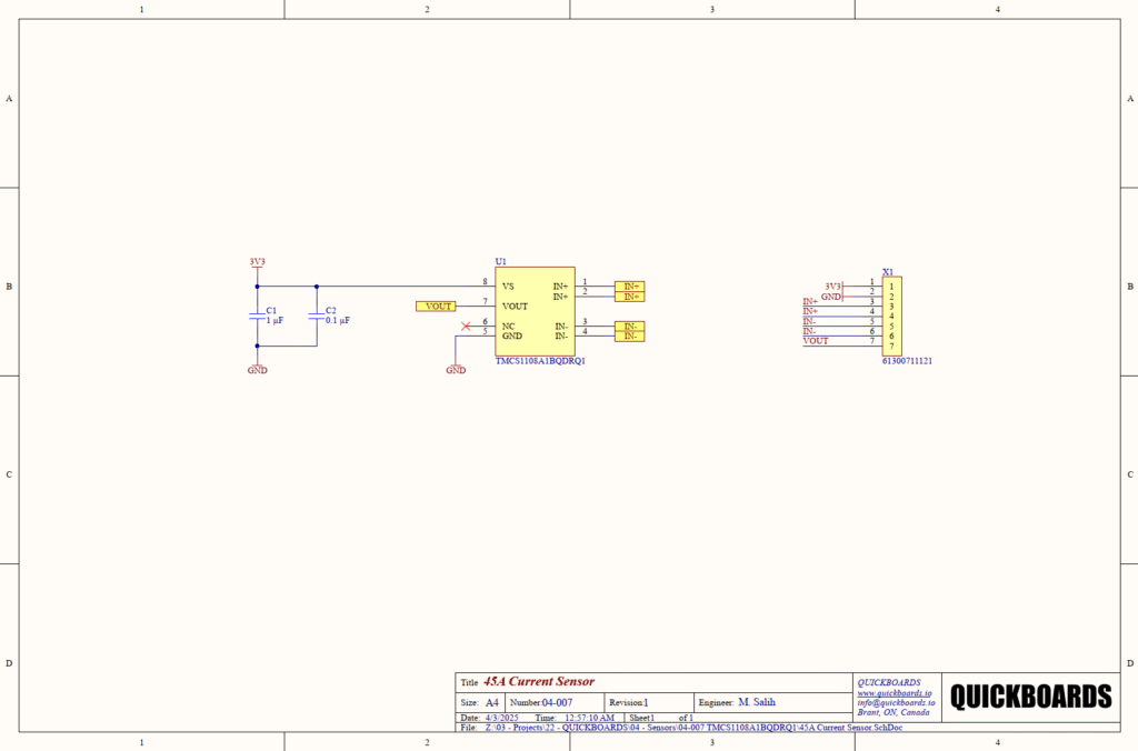
The supply node (VS) at pin 8 is supported by a dual-capacitor decoupling network consisting of C1 (1 uF) and C2 (0.1 uF). Hall-effect sensors are sensitive to supply noise, which can manifest as jitter or offset in the analog output. C2 is a high-frequency bypass capacitor, chosen for its low equivalent series inductance (ESL) to filter out fast switching transients from nearby digital logic. C1 provides localized bulk energy storage to stabilize the internal amplifier during load steps. Ceramic X7R capacitors are specified here for their superior thermal stability and aging characteristics compared to standard electrolytic types.
High-Current Sensing Path
The high-power signal enters through pins 1 and 2 (IN+) and exits through pins 3 and 4 (IN-). The internal lead-frame conductor has an extremely low resistance of 0.5 mOhms. This design choice is fundamental to minimizing power dissipation ($P = I^2 \times R$) and subsequent self-heating at the 45A rating. In the provided schematic, these pins are broken out to a high-density connector (X1). Senior engineers must ensure that the PCB traces connected to these pins utilize heavy copper (2 oz or 3 oz) and wide pours to prevent the PCB itself from becoming the primary source of thermal rise.
Signal Output Logic
The VOUT pin (Pin 7) provides a ratiometric analog voltage. In this bi-directional sensing configuration, the output is centered at VS / 2 during zero-current conditions. The trace logic for VOUT should be kept as short as possible to minimize capacitive loading, which can affect the 80 kHz bandwidth of the sensor. The schematic routes this signal directly to the breakout header for system-level integration with a host microcontroller’s analog front-end.
Placement & Trace Logic
Physical placement of the TMCS1108A1BQDRQ1 is governed by isolation requirements. The IC should be placed such that a physical “moat” or keep-out area exists between the primary current side (pins 1-4) and the secondary signal side (pins 5-8). For 45A operation, thermal relief vias should be avoided on the high-current pads; instead, a solid solder connection to a large copper plane is required to help pull heat away from the IC package.
Implementation Insights
When integrating this block into a larger system, the ratiometric nature of the output must be accounted for in firmware. Because VOUT scales with VS, any drift in the 3.3V regulator will translate directly into a measurement error. Using a high-precision LDO to power the sensor, or sharing the same reference voltage between the sensor and the ADC, is required to maintain the specified 1 percent accuracy.
Magnetic interference is another critical factor. External magnetic fields from nearby transformers, inductors, or high-current busbars can induce a parasitic field in the sensor’s Hall element. To mitigate this, the sensor should be placed away from high-switching magnetic components or oriented such that the sensing axis is perpendicular to external fields.
Finally, thermal management is a primary concern at 45A continuous loads. Although the internal resistance is low, the small SOIC-8 footprint has a finite thermal resistance ($R_{theta JA}$). If the design requires sustained 45A operation, active cooling or thermal interface materials may be necessary to keep the junction temperature within safe limits.
Applications
- Electric Vehicle (EV) Charging: Monitoring AC and DC current in residential and commercial chargers for billing and safety.
- Motor Control: Phase current sensing in brushless DC (BLDC) motors for torque and speed control loops.
- Solar Inverters: Tracking string currents and inverter output to optimize power conversion efficiency.
- Battery Management Systems (BMS): High-side current monitoring for state-of-charge (SoC) and state-of-health (SoH) calculations in lithium-ion packs.
- Uninterruptible Power Supplies (UPS): Real-time monitoring of battery discharge and load distribution in data center environments.
Integrating the TMCS1108A1BQDRQ1 into your design
The TMCS1108A1BQDRQ1 modular block provides a validated, production-ready solution for high-power current monitoring. By utilizing the pre-tested decoupling strategy and optimized pin mapping, engineers can bypass the complexities of isolation coordination and precision analog design. This building block ensures that the sensor operates at its peak accuracy while maintaining the necessary safety barriers between high-voltage buses and sensitive control logic.
Skip the tedious research and manual entry. Download the production-ready schematic block for the TMCS1108A1BQDRQ1 directly from the Quickboards Library.