PIC24FJ128GA006 Reference Schematic Design
The PIC24FJ128GA006 is a high-performance 16-bit microcontroller from Microchip’s PIC24F family, designed to bridge the gap between 8-bit MCUs and 32-bit digital signal controllers. It is built on a modified Harvard architecture and is favored for applications requiring moderate computational power, expansive I/O availability, and low power consumption. This IC is frequently found in industrial controllers, medical monitoring devices, and sophisticated consumer electronics where deterministic performance and robust peripheral sets are mandatory.
Overview of the PIC24FJ128GA006
The device features 128 KB of Flash program memory and 8 KB of RAM, making it suitable for applications with complex firmware requirements. Its integration of a 10-bit Analog-to-Digital Converter (ADC) with up to 16 channels and multiple serial communication interfaces allows it to act as a central hub for sensor data acquisition and system management.
| Feature | Specification |
| Core Architecture | 16-bit PIC24 |
| Max CPU Speed | 32 MHz (16 MIPS) |
| Operating Voltage | 2.0V to 3.6V |
| Program Memory | 128 KB Flash |
| RAM | 8 KB |
| ADC | 10-bit, 500 ksps, 16-ch |
| Communication | 2x UART, 2x SPI, 2x I2C |
| Timers | 5x 16-bit Timers |
| Package | 64-pin TQFP |
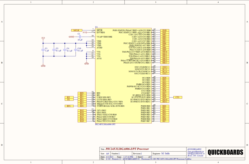
Pin Configuration and Function Mapping
The PIC24FJ128GA006 offers high pin-count flexibility, with many pins multiplexed between general-purpose I/O (GPIO) and specialized hardware peripherals.
| Pin Number | Primary Function | Secondary / Peripheral Functions |
| 7 | MCLR | Master Clear (Reset) Input |
| 10, 26, 38 | VDD | Positive Supply for Peripheral Logic |
| 19 | AVDD | Positive Supply for Analog Peripherals |
| 20 | AVSS | Ground Reference for Analog Peripherals |
| 56 | VCAP/VDDCORE | CPU Core Voltage Filter Capacitor |
| 39, 40 | OSC1 / OSC2 | External Crystal/Oscillator Input |
| 17, 18 | PGC1 / PGD1 | ICSP Programming Clock and Data |
| 34, 33 | U1RX / U1TX | UART1 Receive and Transmit |
| 21-30, 41-44 | RB0 – RB15 | Port B GPIO / ADC Inputs / CN |
| 58-61 | RF0 – RF3 | Port F GPIO / UART / SPI |
Functional Block Analysis & Design Decisions
Power and Decoupling Strategy
The schematic employs a comprehensive decoupling network consisting of 1uF (C1) and 0.1uF (C3, C4, C10) ceramic capacitors. The 0.1uF capacitors are selected for their low Equivalent Series Resistance (ESR) at high frequencies, effectively filtering out synchronous switching noise near the VDD pins. The 1uF capacitor provides a local energy reservoir to handle lower-frequency transients. These must be placed as physically close to the VDD/VSS pin pairs as possible to minimize trace inductance. Additionally, a 10uF high-quality ceramic capacitor (C2) is connected to the VCAP/VDDCORE pin (Pin 56). This is a critical design choice; the PIC24F features an internal voltage regulator to power the 2.5V core. This capacitor stabilizes the regulator and must have low ESR (typically less than 500 mOhms) to ensure CPU stability.
Timing and Oscillation
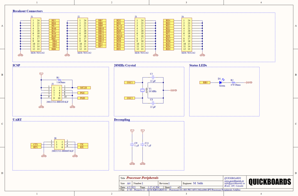
The clock circuit utilizes a 20MHz crystal (Y1) flanked by 22pF load capacitors (C5, C8). The choice of 22pF satisfies the required load capacitance (CL), calculated by the formula CL = (C5 * C8) / (C5 + C8) + Cstray. Using C0G/NP0 ceramic capacitors is recommended here due to their high thermal stability, ensuring the clock frequency does not drift with temperature. Traces between the crystal and the OSC pins must be kept short and symmetrical to reduce EMI radiation.
In-Circuit Serial Programming (ICSP)
The programming interface is broken out via J5, utilizing a 10-pin header. A 1kOhm resistor (R1) is placed on the MCLR line. This acts as a pull-up to VDD to prevent accidental resets during normal operation, while allowing the programmer to pull the line low or high during flash cycles. The inclusion of dedicated PGC and PGD lines ensures the device can be debugged and programmed in-system without interfering with other digital peripherals.
User Interface and I/O Breakout
A status LED (D1) is connected to RB3 through a 470 Ohm current-limiting resistor (R2). At a 3.3V logic level, this provides approximately 3-5mA to the LED, ensuring visibility without excessive power drain. The schematic also features four high-density M20 connectors (J1-J4) that breakout nearly all available GPIOs. This modular approach allows the processor block to interface with various daughterboards or sensors.
UART Communication Interface
The UART block (J6) includes hardware flow control signals (CTS/RTS). This is a professional design choice for robust serial communication, as it prevents buffer overflows during high-speed data transfers. These lines are essential when interfacing with modules where data bursts can exceed the MCU’s immediate processing capacity.
Implementation Insights
When integrating this PIC24F block, it is vital to maintain separate ground paths for analog and digital signals (AVSS and VSS) until a single star-point connection. This prevents digital switching noise from coupling into the sensitive 10-bit ADC.
A frequent oversight is the ESR rating of the VCAP capacitor. If a standard electrolytic capacitor with high ESR is used instead of a low-ESR ceramic or tantalum, the internal core regulator may oscillate, leading to unpredictable CPU resets or brown-out behavior even when the main 3.3V rail is stable.
Applications
- Industrial Automation Controllers: Used for PLC-like logic and sensor monitoring due to high I/O count and robust interrupt handling.
- Medical Diagnostic Equipment: The integrated ADC and low-power modes make it ideal for handheld pulse oximeters or glucose monitors.
- Home Appliance Control: Manages user interfaces, motor control timings, and thermal sensors in white goods.
- Automotive Accessory Modules: Functions well in lighting controllers or dashboard gateways where 16-bit processing is required for CAN bus or LIN bus data management.
Integrating the PIC24FJ128GA006 into your design
This modular block provides a pre-validated foundation for 16-bit embedded systems. By utilizing this reference design, engineers eliminate the uncertainty of core regulator stabilization and oscillator tank circuit tuning. The layout-ready decoupling and standardized ICSP header allow you to focus on your application-specific logic rather than fundamental hardware bring-up.
Skip the tedious research and manual entry. Download the production-ready schematic block for the PIC24FJ128GA006 directly from the Quickboards Library.