ATSAME51N20A Reference Schematic Design
The ATSAME51N20A is a high-performance microcontroller based on the 32-bit ARM Cortex-M4F processor with a Floating Point Unit (FPU). Operating at speeds up to 120 MHz, this device is engineered for complex connectivity and control applications that require robust processing power and extensive peripheral support. It is a staple in industrial automation, automotive gateways, and high-speed data acquisition systems due to its integrated 10/100 Ethernet MAC and dual CAN FD interfaces. The “E” series within the SAM family specifically emphasizes enhanced connectivity and hardware-based security features, making it ideal for secure IoT nodes and networked industrial controllers.
Unlock the Quickboards Library
Get instant access to this Altium Schematic and hundreds of other subcircuits. Hardware design, modularized. Schematic + Layout + Firmware. Built to IPC standards for zero re-spins.
Overview of the ATSAME51N20A
Beyond its raw clock speed, the ATSAME51N20A provides 1024 KB of Flash and 256 KB of SRAM, offering significant headroom for advanced communication stacks and real-time operating systems (RTOS). Its architecture includes a sophisticated Peripheral Touch Controller (PTC) and multiple SERCOM modules that can be dynamically configured for I2C, SPI, or USART communication.
| Feature | Specification |
| Core Architecture | 32-bit ARM Cortex-M4F |
| Max CPU Speed | 120 MHz |
| Operating Voltage | 1.71V to 3.63V |
| Program Memory | 1024 KB Flash |
| RAM | 256 KB SRAM |
| Connectivity | Ethernet MAC, 2x CAN FD |
| ADC | Dual 12-bit, 1 Msps |
| DAC | Dual 12-bit, 1 Msps |
| Package | 100-pin TQFP |
Pin Configuration and Function Mapping
The 100-pin TQFP package allows for an expansive I/O set, enabling simultaneous use of high-speed communication and precise analog peripherals.
| Pin Number | Primary Function | Secondary / Peripheral Functions |
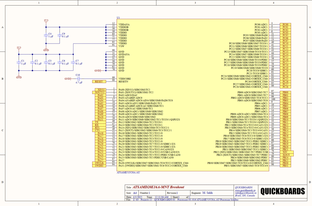
| 12 | VDDANA | Analog Supply Voltage |
| 89 | VDDCORE | Internal Core Regulator Output |
| 91 | VSW | Internal Regulator Switching Node |
| 88 | RESETN | System Reset (Active Low) |
| 93, 94 | SWDCLK / SWDIO | Serial Wire Debug Interface |
| 47, 48 | PA12 / PA13 | SERCOM2 UART TX / RX |
| 78, 79 | PB22 / PB23 | Main Crystal Oscillator (XIN/XOUT) |
| 1, 2 | PA00 / PA01 | 32.768 kHz Crystal (XIN32/XOUT32) |
| 3 | PC00 | GPIO / ADC1 Input |
| 30, 39, 63 | VDDIO | Digital I/O Supply Rails |
Functional Block Analysis & Design Decisions
Power and Decoupling Strategy
The ATSAME51N20A requires a sophisticated power distribution network to maintain signal integrity at 120 MHz. The design utilizes a combination of 1uF (C1) and 0.1uF (C2, C3, C6, C7) ceramic capacitors across the VDDIO rails. For high-speed CMOS devices, the 0.1uF X7R ceramic capacitors provide low-impedance paths for high-frequency switching noise, while the 1uF capacitor serves as a localized energy reservoir for lower-frequency transients. A critical design element is C10, a 4.7uF capacitor on the VDDCORE pin (Pin 89). The internal core of the SAM E51 operates at a lower voltage generated by an internal regulator; this capacitor is mandatory for regulator stability and core logic integrity. All decoupling components must be placed with direct, short traces to their respective VDD/GND pairs to minimize parasitic inductance.
Timing and Oscillation
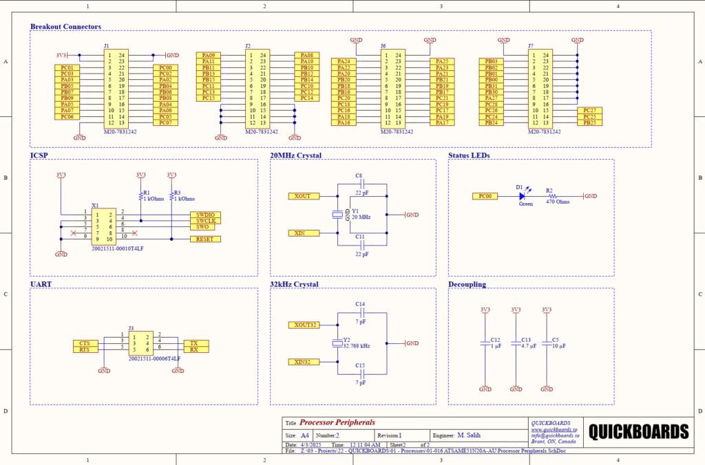
This schematic implements a dual-clock strategy. The primary system clock is driven by a 20MHz crystal (Y1) with 22pF load capacitors (C8, C11). This provides the high-precision reference necessary for the internal Phase-Locked Loop (PLL) to reach 120 MHz and ensure reliable Ethernet and CAN FD timing. Additionally, a 32.768 kHz crystal (Y2) with 7pF capacitors (C14, C15) is used for the Real-Time Clock (RTC) and ultra-low-power sleep modes. The 7pF value is specifically chosen to match the high-impedance requirements of low-power watch crystals, ensuring reliable startup and long-term accuracy.
Programming and Debug Interface
The block utilizes the Serial Wire Debug (SWD) protocol via connector J5. This 10-pin interface provides full hardware debugging and flash programming capabilities while occupying less board real estate than traditional JTAG. 1kOhm pull-up resistors (R1, R3) are placed on the SWDIO and RESETN lines. These define a known logic-high state, preventing environmental electromagnetic interference (EMI) from inducing a floating-input state that could cause unintended resets or interrupt the debug session.
UART and Status Indication
For system telemetry, a UART interface is broken out on J3, including CTS and RTS signals for hardware flow control. Hardware flow control is a senior-level design choice essential for high-speed serial data transfers, preventing buffer overruns when the MCU is busy with high-priority Ethernet or CAN interrupts. A green status LED (D1) is tied to PC00 through a 470 Ohm resistor (R2), providing a visual “heartbeat” for the application firmware.
I/O Breakout and Signal Access
The modular nature of the design is reflected in the four high-density M20 series connectors (J1, J2, J6, J7). These provide access to nearly the entire 100-pin TQFP footprint, allowing the processor block to be easily integrated into a larger carrier board or used for rapid peripheral prototyping.
Implementation Insights
When integrating the ATSAME51N20A, engineers must pay close attention to the VDDANA and GNDANA pins. While this block provides a general-purpose connection, high-precision 12-bit analog applications benefit from isolating the analog ground from the digital ground plane using a star-point connection or a ferrite bead on the supply line to prevent digital switching noise from degrading the ADC’s signal-to-noise ratio.
The internal buck regulator (VSW/VDDCORE) is highly efficient but sensitive to layout. If the buck regulator mode is enabled in software, the placement of the output filter components is critical to prevent the switching frequency from radiating EMI into the surrounding analog traces. If the LDO mode is used instead, ensure the power dissipation remains within the thermal limits of the TQFP package.
Applications
- Industrial IoT Gateways: Utilizes the dual CAN FD and Ethernet MAC to bridge factory floor data to cloud-based monitoring systems.
- Automotive Control Units: The hardware-based CAN FD support makes it suitable for body control modules and diagnostic tools requiring high bandwidth.
- Advanced Motor Control: Integrated 120 MHz FPU and high-speed PWM modules enable real-time Field Oriented Control (FOC) for brushless DC motors.
- Medical Diagnostic Equipment: The high-speed 1Msps ADC and FPU facilitate real-time signal processing for portable monitoring devices.
Integrating the ATSAME51N20A into your design
The ATSAME51N20A modular block streamlines the adoption of high-performance ARM Cortex-M4F processing by handling the foundational hardware requirements of core voltage regulation and dual-clock oscillation. By utilizing this pre-validated schematic, designers can significantly reduce the risk of power-on-reset failures or oscillator instability, focusing their engineering efforts on higher-level system integration and firmware optimization.
Skip the tedious research and manual entry. Download the production-ready schematic block for the ATSAME51N20A directly from the Quickboards Library.