PIC18F67J11T-I/PT Reference Schematic Design
The PIC18F67J11T-I/PT is a high-performance, 8-bit microcontroller from Microchip’s PIC18 family, specifically designed for applications requiring high memory density and extensive I/O capabilities in a cost-effective package. Featuring a J-series architecture, it operates at lower voltages while maintaining high computational throughput, making it an ideal candidate for industrial controllers, handheld medical devices, and communication gateways.
| Feature | Specification |
| Architecture | 8-bit PIC18 (C Compiler Optimized) |
| Program Memory | 128 KB Flash |
| RAM | 3930 Bytes |
| Operating Voltage | 2.0V to 3.6V |
| Max Speed | 48 MHz (12 MIPS) |
| I/O Pins | 54 Pins |
| Peripherals | 2 UART, 2 SPI/I2C, 3 CCP |
| ADC | 11-channel, 10-bit |
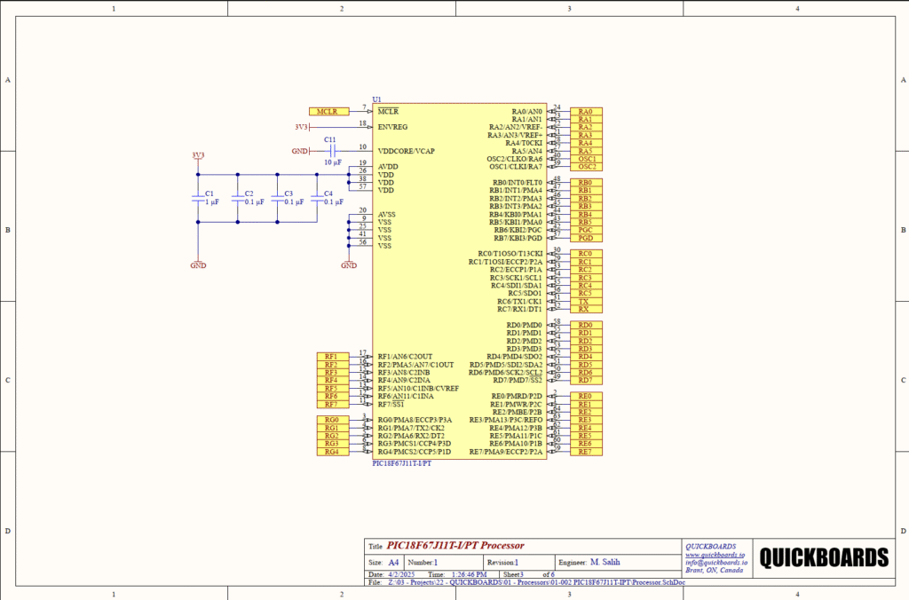
Pin Configuration and Function Mapping
The following table outlines the primary and secondary functions for the core pins utilized in this modular design. This configuration ensures that all essential programming and communication headers are accessible for rapid prototyping.
| Pin Number | Primary Function | Secondary / Peripheral Functions |
| 7 | MCLR | Master Clear (Reset) / Vpp Programming |
| 39, 40 | OSC1, OSC2 | External Crystal Oscillator Input/Output |
| 31, 32 | RC6, RC7 | UART Transmit (TX) / Receive (RX) |
| 37, 42 | RB7, RB6 | ICSP Programming Data (PGD) / Clock (PGC) |
| 10 | VDDCORE/VCAP | Internal Regulator Filter Capacitor Connection |
| 19, 26, 38, 57 | VDD / AVDD | Positive Supply Rails |
| 20, 9, 25, 41, 56 | VSS / AVSS | Ground Reference Rails |
Functional Block Analysis & Design Decisions
Power and Decoupling Strategy
The schematic employs a multi-tier decoupling strategy to ensure power integrity across the high-pin-count device. A 1 muF capacitor (C1) acts as a local bulk reservoir, while multiple 0.1 $\mu$F ceramic capacitors (C2, C3, C4, C7) are distributed across the VDD pins.
- Component Selection: 0.1 muF X7R ceramic capacitors are specified due to their low Equivalent Series Resistance (ESR) and stability over temperature.
- VCAP Regulation: C11 (10 muF) is critical for the internal LDO regulator stability. This should be a low-ESR tantalum or ceramic capacitor to maintain the 1.2V core voltage.
- Placement: Decoupling capacitors must be placed as close as possible to the VDD/VSS pairs to minimize inductive loops.
Timing and Oscillation
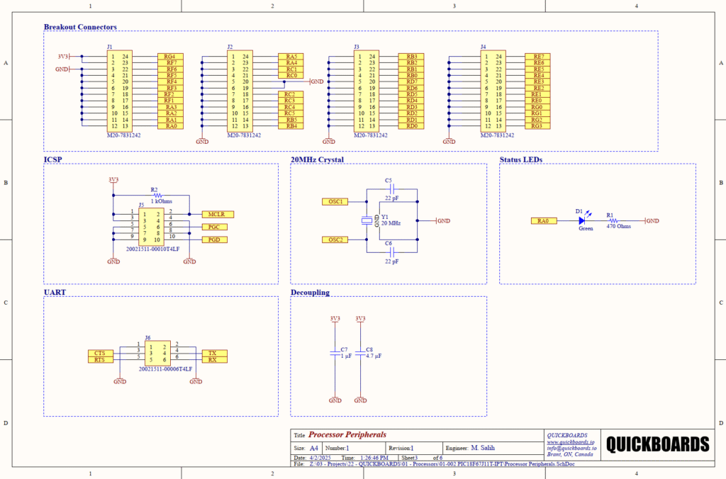
The timing circuit utilizes a 20 MHz Crystal (Y1) flanked by two 22 pF load capacitors (C5, C6).
- Design Rationale: The 22 pF value is chosen to match the typical load capacitance requirements of high-frequency crystals, ensuring the oscillator starts reliably and maintains a stable frequency.
- Trace Logic: The OSC1 and OSC2 traces should be short, symmetrical, and isolated from high-speed digital signals by a ground guard ring to prevent EMI injection.
ICSP Programming Interface
The In-Circuit Serial Programming (ICSP) block (J5) facilitates firmware deployment and debugging.
- Signal Conditioning: R2 (10 kOhm) serves as a pull-up resistor on the MCLR line. This defines the default state as “Not Reset” while allowing the programmer to pull the line low.
- Isolation: No high-value capacitors should be placed on the MCLR line, as they can interfere with the fast-rising edges required by the PICkit or ICD programmers.
UART Communication
The UART block (J6) provides a standard asynchronous serial interface.
- Design Rationale: The TX and RX lines are broken out for serial communication. While the schematic shows direct connections, the integration of 0 Ohm series resistors is often considered for EMI tuning, though omitted here for simplicity in a standard digital block.
Status Indication
A single Green LED (D1) is mapped to RA0 for visual diagnostics.Component Selection: R1 (470 Ohm) limits the current to approximately 3 mA (assuming a 1.8V forward voltage drop at 3.3V VDD), which is sufficient for visibility while remaining well within the 25 mA source limit of the PIC18 I/O port.
Implementation Insights
For a 64-pin TQFP device, maintaining a continuous ground plane is essential for signal integrity. Engineers should avoid routing long traces that “split” the ground return path under the MCU, as this significantly increases radiated emissions and susceptibility to external noise. Because the PIC18F67J11T is not 5V tolerant on most pins, it is vital to ensure all peripheral logic for UART and breakout headers operates at 3.3V to prevent permanent damage to the silicon. Finally, all unused I/O pins should be configured as outputs and driven low in software, or pulled to VDD or VSS via resistors, to prevent floating CMOS inputs from increasing idle power consumption.
Applications
- Industrial Data Loggers: High Flash memory capacity allows for extensive local buffering of sensor data before transmission to a central server.
- Handheld Medical Devices: The low power J-series architecture extends battery life in portable diagnostic equipment and patient monitors.
- Embedded Web Servers: Dual UART and SPI interfaces facilitate the integration of Ethernet or Wi-Fi modules for IoT-ready industrial applications.
- Motor Control: Built-in Capture/Compare/PWM modules enable precise control of DC motors or actuators in automation systems.
Integrating the PIC18F67J11T into your design
The PIC18F67J11T modular block provides a validated foundation for high-density 8-bit processing. By utilizing this pre-tested subcircuit, you ensure that critical power sequencing, clock stability, and programming interfaces are correctly implemented from day one. This reduces the risk of hardware failure and allows the engineering team to focus on application-specific firmware and sensor integration rather than troubleshooting basic silicon requirements.
Skip the tedious research and manual entry. Download the production-ready schematic block for the PIC18F67J11T directly from the Quickboards Library.