MCP3202T-CI/SN 12bit Analog to Digital Converter Reference Schematic Design
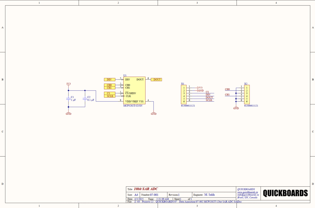
The MCP3202T-CI/SN is a high-performance 12-bit Successive Approximation Register (SAR) Analog-to-Digital Converter (ADC) that features two analog input channels and an industry-standard SPI serial interface. While the provided schematic title block refers to a 10-bit device, the MCP3202 is natively a 12-bit converter, providing significantly higher granularity for precision measurements. This IC is typically employed in applications requiring a balance of low power consumption and high resolution, such as instrumentation, sensor monitoring, and portable data logging.
Overview of the MCP3202T-CI/SN
This converter allows for either two single-ended inputs or a single pseudo-differential pair, giving designers flexibility in how they interface with analog front-ends. By utilizing a SAR architecture, the device provides low latency and deterministic conversion times. Its low active current makes it ideal for remote or battery-powered sensor nodes where power budgets are strictly managed.
| Feature | Specification |
| Resolution | 12-bit |
| Number of Channels | 2 |
| Interface Type | SPI (Modes 0,0 and 1,1) |
| Operating Voltage | 2.7V to 5.5V |
| Max Sampling Rate | 100 ksps (at 5V) / 50 ksps (at 2.7V) |
| Architecture | SAR |
| Standby Current | 500 nA (typical) |
| Active Current | 550 uA (max at 5V) |
Pin Configuration and Function Mapping
The MCP3202 operates in an 8-pin package, maximizing functionality while minimizing the physical footprint on the PCB.
| Pin Number | Primary Function | Secondary / Peripheral Functions |
| 1 | CS/SHDN | Chip Select / Shutdown Input |
| 2 | CH0 | Analog Input Channel 0 |
| 3 | CH1 | Analog Input Channel 1 |
| 4 | VSS | Ground Reference |
| 5 | DIN | Serial Data Input |
| 6 | DOUT | Serial Data Output |
| 7 | CLK | Serial Clock Input |
| 8 | VDD/VREF | Power Supply and Analog Reference |
Functional Block Analysis & Design Decisions
Power and Decoupling Strategy
The design utilizes a 3.3V supply rail (3V3) connected to Pin 8, which serves as both the analog supply and the voltage reference (VREF). This simplifies the bill of materials by eliminating the need for a dedicated reference IC, though it necessitates a very clean supply rail. The decoupling network consists of a 1 uF (C1) and a 0.1 uF (C2) capacitor. The 0.1 uF capacitor is selected for its superior performance in filtering high-frequency noise due to its low equivalent series inductance. The 1 uF capacitor provides bulk stability and handles lower-frequency transients. Ceramic X7R capacitors are specified here because they offer an excellent balance of high capacitance per volume and thermal stability compared to electrolytic or Y5V alternatives. These capacitors must be placed as close to Pin 8 as physically possible to minimize parasitic trace inductance.
Analog Input Interface
Pins 2 and 3 (CH0 and CH1) are routed to the X2 connector. In SAR ADCs, the input must charge an internal sampling capacitor during the acquisition phase. Consequently, the source impedance of the analog signal is critical. For this 12-bit system to maintain accuracy, the driving circuit should have a low output impedance. If a high-impedance sensor is used, an external operational amplifier configured as a buffer is recommended to prevent gain errors. The schematic routes these signals directly to headers, allowing for the addition of external anti-aliasing filters which are necessary to prevent high-frequency noise from aliasing into the baseband during conversion.
Digital Interface Logic
The digital communication block utilizes an SPI interface broken out to the X1 connector. This include DIN, DOUT, CLK, and CS/SHDN. The CS/SHDN pin serves a dual purpose: it initiates communication and puts the device into a low-power shutdown mode when high. This allows for effective power management in multi-sensor systems. The traces for the SPI clock (CLK) and data lines should be kept relatively short and isolated from the analog input traces (CH0/CH1) to prevent digital switching noise from coupling into the sensitive analog measurements.
Implementation Insights
When integrating the MCP3202 block, the quality of the 3.3V rail is paramount. Since VDD and VREF are tied, any ripple on the power supply will translate directly into measurement error. Senior engineers will often place a ferrite bead in series with the 3V3 rail before the decoupling capacitors to further isolate the ADC from digital noise on the main power plane.
A significant consideration for SAR ADCs is the grounding strategy. A solid ground plane is highly recommended. The VSS pin (Pin 4) should have a direct, low-impedance path to the ground plane. Splitting analog and digital grounds is generally unnecessary for a 12-bit device of this speed, provided that the digital return paths are kept away from the sensitive analog inputs to avoid ground bounce issues.
Applications
- Sensor Interface: Digitizing analog outputs from temperature, pressure, or humidity sensors.
- Process Control: Monitoring industrial signal loops, such as 4-20mA or 0-10V systems, through appropriate attenuation.
- Data Acquisition: General-purpose logging of analog voltages in modular embedded systems.
- Battery Monitoring: Measuring individual cell voltages in portable or remote power management units.
Integrating the MCP3202T-CI/SN into your design
This modular block provides a pre-validated hardware foundation for 12-bit analog-to-digital conversion, ensuring that critical decoupling and pin mapping are handled correctly. By utilizing this sub-system, you eliminate the repetitive task of configuring core support circuitry, allowing you to focus on signal conditioning and firmware-level data processing.
Skip the tedious research and manual entry. Download the production-ready schematic block for the MCP3202T-CI/SN directly from the Quickboards Library.