DSPIC33EP256MU806 Reference Schematic Design
The DSPIC33EP256MU806 is a high-performance 16-bit Digital Signal Controller (DSC) from Microchip, specifically engineered to combine the control capabilities of a microcontroller with the computation power of a Digital Signal Processor (DSP). This device is a cornerstone for applications requiring high-speed deterministic performance, such as motor control, power conversion, and advanced sensor processing. Its architecture is optimized for execution of complex mathematical algorithms, making it an ideal candidate for real-time control loops in industrial and automotive environments.
Overview of the DSPIC33EP256MU806
Operating at speeds up to 70 MIPS, the DSPIC33EP256MU806 features a specialized DSP engine with a single-cycle MAC (Multiply-Accumulate) and dual 40-bit accumulators. This hardware acceleration allows it to handle intensive signal processing tasks that would overwhelm standard 16-bit MCUs. With 256 KB of Flash and integrated peripherals like USB 2.0 OTG and multiple high-speed PWM generators, it serves as a highly integrated solution for complex mechatronic systems.
| Feature | Specification |
| Core Architecture | 16-bit dsPIC33E (70 MIPS) |
| Operating Voltage | 3.0V to 3.6V |
| Program Memory | 256 KB Flash |
| RAM | 28 KB |
| USB | USB 2.0 OTG Full Speed |
| ADC | 10-bit/12-bit, up to 1.1 Msps |
| Timers | Up to 9x 16-bit or 4x 32-bit |
| Communication | 2x UART, 2x SPI, 2x I2C, CAN |
| Package | 64-pin TQFP |
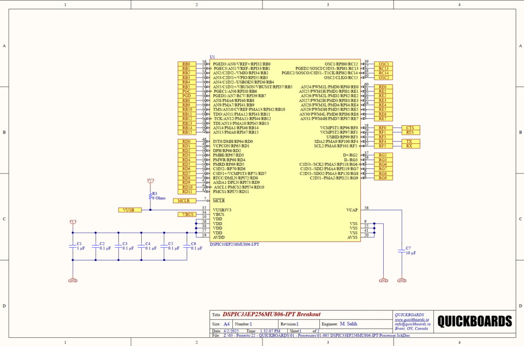
Pin Configuration and Function Mapping
The 64-pin TQFP package provides a dense array of I/O, many of which support Remappable Peripheral Pin (RPP) technology, allowing for flexible PCB routing.
| Pin Number | Primary Function | Secondary / Peripheral Functions |
| 7 | MCLR | Master Clear / Programming Voltage |
| 10, 26, 38, 57 | VDD | Digital Logic Power (3.3V) |
| 19 | AVDD | Analog Power Supply |
| 20 | AVSS | Analog Ground Reference |
| 56 | VCAP | Core Voltage Regulator Filter Pin |
| 39, 40 | OSC1 / OSC2 | Main Oscillator / Crystal Inputs |
| 21, 22 | PGED1 / PGEC1 | ICSP Data and Clock |
| 4, 5 | RF5 / RF4 | UART1 RX and TX |
| 58, 59 | RF0 / RF1 | UART1 CTS and RTS |
| 34, 35 | VBUS / VUSB3V3 | USB Power and Internal Regulator |
Functional Block Analysis & Design Decisions
Power and Decoupling Strategy
The power system for this DSC utilizes a multi-tier decoupling strategy to maintain rail stability during high-speed DSP operations. The design implements a bulk 1uF capacitor (C1) alongside five 0.1uF capacitors (C2, C3, C4, C5, C6). Using multiple 0.1uF ceramic capacitors distributed across the VDD pins is standard for mitigating high-frequency noise caused by synchronous logic switching. For the internal 1.8V core regulator, a 10uF low-ESR ceramic capacitor (C7) is connected to the VCAP pin (Pin 56). This value is non-negotiable for stability; a lower value or high-ESR type can lead to core logic jitter and unexpected resets.
Timing and Oscillation
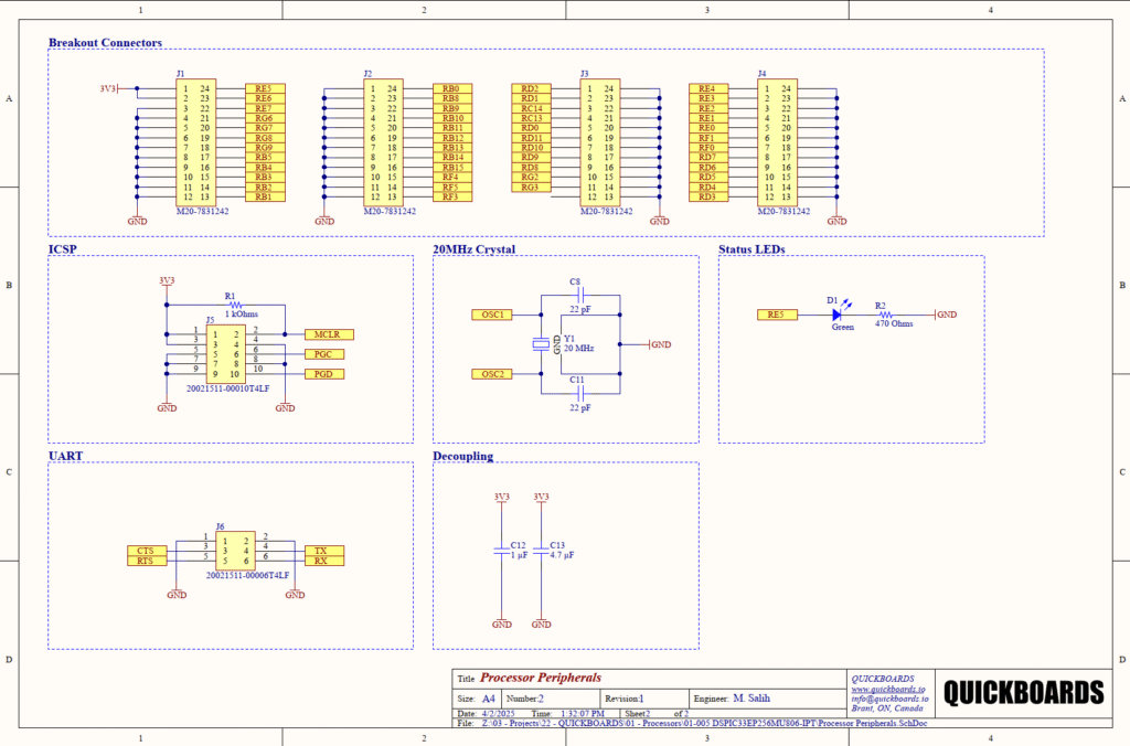
The timing block is centered around a 20MHz crystal (Y1) with 22pF load capacitors (C8, C11). This 20MHz reference is typical for dsPIC33E designs, as it provides a stable base for the internal PLL to scale the system clock up to 140MHz (yielding 70 MIPS). The capacitors use C0G dielectric to ensure frequency stability across a wide temperature range. To minimize parasitic capacitance and EMI, these components must be placed as close to Pins 39 and 40 as possible, with a ground plane directly underneath the crystal.
Programming and Debugging (ICSP)
The ICSP interface (J5) is designed for seamless integration with production programmers. A 1kOhm resistor (R1) serves as a pull-up on the MCLR line to VDD, preventing accidental resets while remaining high-impedance enough for the programmer to drive the line for entry into debug mode. This configuration avoids the need for a physical reset button while maintaining reliable operation in electrically noisy environments.
UART and Flow Control
The UART interface (J6) includes dedicated RTS and CTS signals. In signal processing applications, the data throughput can be extremely high; hardware flow control is implemented to ensure that the serial buffer does not overflow when the DSP engine is occupied with high-priority math interrupts. The lines are broken out through an industry-standard 6-pin header for easy interfacing with external modules or PC-link cables.
User Feedback and Breakout
A status LED (D1) is driven by RE5 through a 470 Ohm resistor (R2). This provides a simple diagnostic tool for software “heartbeat” signaling. The entire peripheral set is made accessible through high-density M20 breakout connectors (J1-J4), allowing the module to be treated as a plug-and-play processor core for larger system integration.
Implementation Insights
A critical consideration for the dsPIC33E family is the AVDD/AVSS connection. Even if the ADC is not used, AVDD must be connected to 3.3V and AVSS to GND for the chip to function correctly. Senior engineers should note that the internal USB regulator (VUSB3V3) requires the VBUS pin to be powered or tied to 3.3V via a 0 Ohm resistor (R3) if the USB peripheral is utilized, as seen in this design.
One common oversight is the routing of the VCAP capacitor. This pin is the only source of stability for the internal core; the ground return path for C7 should be as direct as possible to the VSS pins to minimize the loop area of the core voltage regulator.
Applications
- Digital Power Supplies: Used in DC/DC converters and Inverters where the high-speed PWM and DSP engine manage complex switching cycles.
- AC Induction Motor Control: Handles Field Oriented Control (FOC) algorithms and sensorless vector control with high precision.
- Industrial Sensor Hubs: Ideal for processing analog signals from strain gauges or pressure sensors where 12-bit ADC accuracy and filtering are required.
- Automotive Control Units: Suitable for auxiliary functions like climate control or seat positioning where CAN communication and robust temperature operation are necessary.
Integrating the DSPIC33EP256MU806 into your design
This modular block simplifies the integration of a powerful Digital Signal Controller by providing a pre-validated layout for the most sensitive circuits: the power core and the high-speed oscillator. By adopting this production-ready sub-circuit, engineers can bypass the complexities of core regulator stability and focus directly on their signal processing algorithms and control logic.
Skip the tedious research and manual entry. Download the production-ready schematic block for the DSPIC33EP256MU806 directly from the Quickboards Library.