ATTINY24A Reference Schematic Design
The ATTINY24A is a high-performance, low-power Microchip 8-bit AVR RISC-based microcontroller. It is designed to provide a compact and efficient solution for applications that require a small footprint without sacrificing a robust peripheral set. By executing powerful instructions in a single clock cycle, the device achieves throughputs approaching 1 MIPS per MHz, allowing the system designer to optimize power consumption versus processing speed. It is typically utilized in automotive electronics, consumer appliances, and industrial control systems where board space is at a premium.
Overview of the ATTINY24A
The ATTINY24A features 2 KB of in-system programmable Flash, 128 bytes of EEPROM, and 128 bytes of SRAM. Despite its small 14-pin count, it integrates a 10-bit ADC, universal serial interface (USI), and multiple timers. This makes it an excellent choice for distributed sensing or as a co-processor in larger modular systems.
| Feature | Specification |
| Core Architecture | 8-bit AVR RISC |
| Operating Voltage | 1.8V to 5.5V |
| Max Operating Frequency | 20 MHz |
| Program Memory | 2 KB Flash |
| RAM / EEPROM | 128 B / 128 B |
| ADC | 10-bit, 8-channel |
| Timers | 1x 8-bit, 1x 16-bit |
| Package | 14-pin SOIC |
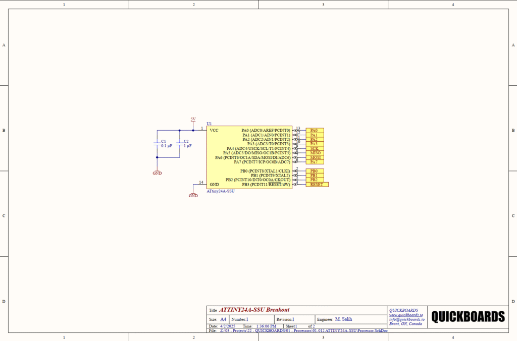
Pin Configuration and Function Mapping
The ATTINY24A maximizes functional density through extensive pin multiplexing, allowing a single pin to serve as a digital I/O, an analog input, or a communication interface.
| Pin Number | Primary Function | Secondary / Peripheral Functions |
| 1 | VCC | Digital Supply Voltage |
| 14 | GND | Ground |
| 13 – 10 | PA0 – PA3 | ADC0-ADC3 / PCINT0-PCINT3 |
| 9 – 7 | PA4 – PA6 | USCK / DO / DI / ADC4-ADC6 |
| 6 | PA7 | ADC7 / OC0B / PCINT7 |
| 2, 3 | PB0, PB1 | XTAL1 / XTAL2 / PCINT8-PCINT9 |
| 5 | PB2 | INT0 / OC0A / PCINT10 |
| 4 | PB3 | RESET / dW / PCINT11 |
Functional Block Analysis & Design Decisions
Power and Decoupling
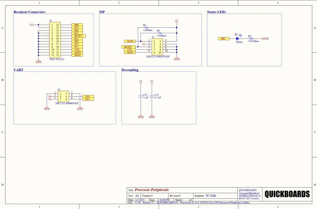
The power block utilizes a dual-capacitor decoupling strategy consisting of 0.1uF (C1) and 1uF (C2) ceramic capacitors. The 0.1uF capacitor is chosen for its low inductance at high frequencies, effectively filtering out high-frequency switching noise, while the 1uF capacitor provides a larger energy reservoir to stabilize the 5V rail against lower-frequency transients. For high-speed digital designs, these must be placed as close to the VCC (Pin 1) and GND (Pin 14) pins as possible to minimize parasitic loop inductance. The peripheral page further supplements this with C12 (1uF) and C13 (4.7uF) to ensure a clean supply across the entire modular board.
Programming Interface (ISP)
The In-System Programming (ISP) block (J2) utilizes a standard 10-pin header. A critical design choice is the inclusion of R3 (1kOhm) as a pull-up on the RESET line. This ensures the microcontroller does not undergo spurious resets in noisy environments. Additionally, R1 (1kOhm) is placed on the MOSI line as an isolation or current-limiting measure, ensuring signal integrity during programming. The layout should ensure that ISP signal traces are of equal length where possible to avoid timing skew during high-speed programming.
Status Indication
A green status LED (D1) is tied to PB0 through a 470 Ohm current-limiting resistor (R2). At a 5V supply, this resistor value limits the forward current to approximately 6-8mA (depending on the LED’s forward voltage drop), which is sufficient for high visibility without exceeding the I/O pin’s maximum source current ratings. This provides an essential “heartbeat” indicator for firmware verification.
UART Communication Interface
Although the ATTINY24A lacks a hardware-dedicated UART, the interface is implemented via pins PA0 and PA1 on connector J3. This modular design allows for software-based UART communication, a standard technique for low-pin-count MCUs. The connector is placed near the edge of the breakout to facilitate easy connection to external serial-to-USB converters for debugging and data logging.
Breakout and Expansion
The breakout connector J1 (M20 series) provides comprehensive access to all I/O pins. In this design, the VCC rail and multiple ground pins are interleaved to provide a low-impedance path and reference for external sensors or daughterboards.
Implementation Insights
When integrating the ATTINY24A, it is essential to consider the clock source. While the internal RC oscillator suffices for low-speed tasks, applications requiring precise timing (like software-serial communication) should utilize the PB0/PB1 pins for an external crystal.
A common oversight involves the shared functionality of the RESET pin. If the RSTDISBL fuse is programmed to use PB3 as general I/O, high-voltage serial programming is required to regain access to the chip. For modular flexibility, it is recommended to keep PB3 as a dedicated reset pin unless I/O requirements are absolute.
Applications
- Sensor Signal Conditioning: Utilizing the 10-bit ADC to pre-process analog signals before sending data to a primary processor.
- Handheld Consumer Electronics: Providing user interface logic and battery monitoring in devices with strict power and size constraints.
- Industrial Lighting Control: Managing PWM dimming cycles for LED arrays based on ambient light sensor inputs.
- Automotive Interior Modules: Controlling small-scale actuators or seat-belt tensioner sensors within the vehicle cabin.
Integrating the ATTINY24A into your design
This modular block simplifies the design process by providing a pre-validated, stable power and programming foundation for the ATTINY24A. By utilizing this subcircuit, engineers can eliminate the risk of power instability or reset-line noise interference, accelerating the path from prototype to production-ready hardware.
Skip the tedious research and manual entry. Download the production-ready schematic block for the ATTINY24A directly from the Quickboards Library.