ATSAMD20E16A Reference Schematic Design
The ATSAMD20E16A is a low-power, high-performance 32-bit microcontroller based on the ARM Cortex-M0+ processor architecture. This IC is designed to provide a flexible and easy-to-use solution for a wide range of embedded applications, balancing computational efficiency with minimized power consumption. It is frequently employed in home automation, industrial control, and consumer medical devices where a compact footprint and high peripheral integration are essential. The device features 64 KB of Flash memory and 8 KB of SRAM, making it an excellent choice for modern sensor-to-cloud interfaces.
Overview of the ATSAMD20E16A
At the heart of the ATSAMD20E16A is the 32-bit ARM Cortex-M0+ CPU, operating at frequencies up to 48 MHz. A standout feature of this family is the Serial Communication Interface (SERCOM), which allows each of its four modules to be configured as an I2C, SPI, or USART interface, providing engineers with exceptional routing flexibility on the PCB.
| Feature | Specification |
| Core Architecture | 32-bit ARM Cortex-M0+ |
| Max CPU Speed | 48 MHz (2.14 CoreMark/MHz) |
| Operating Voltage | 1.62V to 3.63V |
| Program Memory | 64 KB Flash |
| RAM | 8 KB SRAM |
| SERCOM Modules | 4 (Configurable USART, SPI, I2C) |
| ADC | 12-bit, 350 ksps (up to 10 channels) |
| DAC | 10-bit, 350 ksps (1 channel) |
| Package | 32-pin VQFP/TQFP |
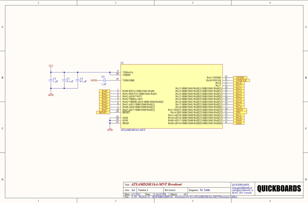
Pin Configuration and Function Mapping
The ATSAMD20E16A utilizes a high degree of pin multiplexing. The table below highlights the primary and peripheral mapping for the pins used in this specific modular block.
| Pin Number | Primary Function | Secondary / Peripheral Functions |
| 30 | VDDIN | Main Digital Supply Rail |
| 9 | VDDANA | Analog Supply Rail |
| 29 | VDDCORE | Internal LDO Output (Core Voltage) |
| 31, 32 | SWDCLK / SWDIO | Serial Wire Debug Programming Interface |
| 26 | RESET | External System Reset |
| 15, 16 | XIN / XOUT | External Crystal Oscillator Input/Output |
| 1 | PA00 | GPIO / SERCOM1 PAD0 / External Interrupt |
| 12, 13 | PA10 / PA11 | GPIO / SERCOM0/2 PAD2/3 (UART RX/TX) |
| 10, 28, 33 | GND / EPAD | System Ground / Exposed Thermal Pad |
Functional Block Analysis & Design Decisions
Power and Decoupling Strategy
The power sub-circuit is designed to ensure a stable operating environment for both the digital core and the sensitive analog peripherals. The main 3V3 rail is decoupled at the source with a 1uF (C1) and two 0.1uF (C2, C3) ceramic capacitors. The 0.1uF capacitors are selected for their low Equivalent Series Resistance (ESR) to filter high-frequency switching noise, while the 1uF capacitor handles lower-frequency ripple. A critical component in this block is C4 (1uF), connected to the VDDCORE pin. The ATSAMD20 features an internal regulator that drops the input voltage down to approximately 1.2V for the CPU core. C4 must be placed as close to Pin 29 as possible to stabilize this regulator and ensure internal logic integrity.
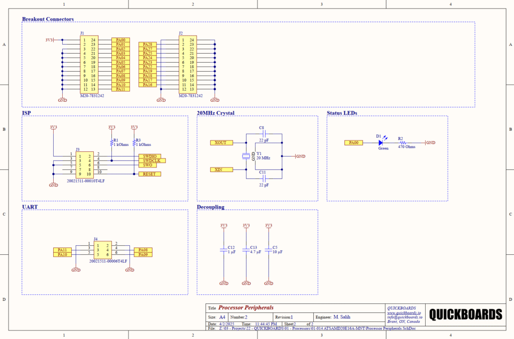
Timing and Oscillation
System timing is provided by a 20MHz crystal (Y1) with 22pF load capacitors (C8, C11). The load capacitance is chosen based on the crystal’s specifications to ensure stable oscillation. For 32-bit ARM MCUs, keeping the oscillator traces short and shielded by a surrounding ground guard ring is standard practice to prevent clock jitter. While the IC includes an internal RC oscillator, the external crystal is implemented here to provide the precision required for reliable high-speed UART and synchronous communication.
Programming and Debug Interface
The schematic utilizes the Serial Wire Debug (SWD) protocol via J3. Unlike older JTAG interfaces, SWD requires only two signals (SWDIO and SWDCLK), saving valuable board space. R1 (1kOhm) serves as a pull-up on the SWDIO line to define its state when the debugger is not connected, while R3 (1kOhm) provides a pull-up for the RESET line. Using 1kOhm instead of the standard 10kOhm provides better noise immunity for the reset line in industrial environments, preventing unintended system restarts.
UART and Communication
Communication is broken out via J4, mapped to SERCOM modules on PA08 through PA11. The layout is optimized for UART transmission, with pins PA10 and PA11 serving as the primary RX and TX paths. Because the SERCOM pins are remappable, this block can easily be adapted to SPI or I2C in software without changing the hardware layout, illustrating the modular flexibility of the ATSAMD20 family.
Status Indication and Breakout
A status LED (D1) is tied to PA00 through a 470 Ohm resistor (R2). At 3.3V, this resistor limits current to approximately 3.5mA, which is sufficient for high-efficiency LEDs while remaining well within the GPIO’s source current limits. The I/O breakout is handled by two 24-pin M20 series connectors (J1, J2), allowing for easy integration with breadboards or daughtercards for rapid prototyping.
Implementation Insights
When integrating the ATSAMD20E16A, it is mandatory to connect the Exposed Pad (EPAD) to the ground plane. This is not only for electrical grounding (Pin 33) but also for thermal dissipation. In high-frequency applications, failing to properly ground the EPAD can result in increased EMI and potential ground-bounce issues.
Another engineering consideration is the VDDANA supply. While connected to 3V3 in this general-purpose block, senior engineers should note that VDDANA can be filtered through a ferrite bead if the 12-bit ADC is used for high-precision measurement. This isolates the analog rail from the digital switching noise present on the VDDIN line.
Applications
- Smart Energy and Metering: Used in smart meters and power monitoring tools due to its high-precision ADC and low-power sleep modes.
- Home Automation Systems: Ideal for lighting controllers and smart thermostats where SERCOM flexibility simplifies peripheral sensor integration.
- Industrial Sensor Nodes: Functions as a robust controller for environmental sensors, utilizing the Cortex-M0+ core for local data processing before transmission.
Integrating the ATSAMD20E16A into your design
This reference block provides a pre-validated, modular foundation that handles the complexities of 32-bit core stabilization and high-speed clocking. By utilizing this sub-circuit, you eliminate the common risks associated with internal regulator decoupling and crystal circuit tuning. This allows your team to skip the fundamental hardware bring-up phase and move directly to application firmware development.
Skip the tedious research and manual entry. Download the production-ready schematic block for the ATSAMD20E16A directly from the Quickboards Library.