AD5693RBRMZ 16bit Digital to Analog Reference Schematic Design
The AD5693RBRMZ-RL7 is a low-power, single-channel, 16-bit voltage-output Digital-to-Analog Converter (DAC) from Analog Devices’ nanoDAC+ family. It is designed for applications where high resolution, small footprint, and low power consumption are critical. This IC features a 2.5V, 2 ppm/degree Celsius internal reference, providing a highly stable output without requiring external reference components. Typical applications include process control, data acquisition systems, digital gain and offset adjustment, and portable instrumentation where precision signal generation is mandatory.
Overview of the AD5693RBRMZ-RL7
The AD5693R utilizes a versatile 2-wire serial interface that is compatible with I2C standard, fast, and high-speed modes. Its internal power-on reset circuit ensures that the DAC output powers up to zero scale or midscale and remains there until a valid write takes place. This deterministic behavior is vital in industrial control systems to prevent unintended actuator movement during power-up.
| Feature | Specification |
| Resolution | 16-bit |
| Interface | I2C (up to 3.4 MHz) |
| Supply Voltage | 2.7V to 5.5V |
| Internal Reference | 2.5V (typical) |
| Output Voltage | 0V to VREF or 0V to 2xVREF |
| INL | +/- 2 LSB (typical) |
| Power Consumption | 1.8 mW at 3V |
| Package | 10-lead MSOP |
Pin Configuration and Function Mapping
The AD5693RBRMZ-RL7 uses a compact 10-pin MSOP package, multiplexing digital control and analog precision within a small board area.
| Pin Number | Primary Function | Secondary / Peripheral Functions |
| 1 | VDD | Power Supply Input |
| 2 | VLOGIC | Digital Interface Power Supply |
| 3 | RESET | Hardware Reset (Active Low) |
| 4 | LDAC | Load DAC (Asynchronous update) |
| 5 | GND | Ground Reference |
| 6 | A0 | I2C Address Select Bit |
| 7 | SCL | I2C Serial Clock Input |
| 8 | SDA | I2C Serial Data Input/Output |
| 9 | VREF | Reference Input/Output |
| 10 | VOUT | Analog Output Voltage |
Functional Block Analysis & Design Decisions
Power and Tiered Decoupling
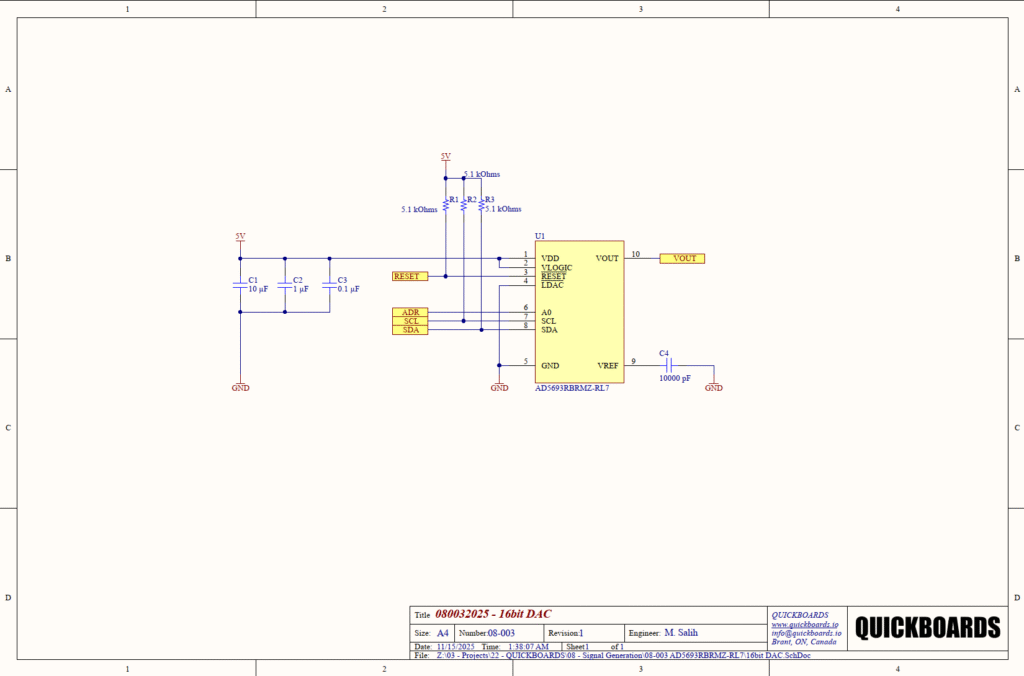
This design utilizes a 5V supply for both VDD and VLOGIC. To ensure high-frequency stability and low-noise performance—essential for a 16-bit converter—a tiered decoupling strategy is implemented using C1 (10uF), C2 (1uF), and C3 (0.1uF). The 0.1uF ceramic capacitor provides a low-impedance path to ground for high-frequency switching noise, while the 10uF capacitor handles bulk energy storage for lower-frequency transients. These should be placed as close to Pin 1 as possible. Ceramic X7R dielectrics are specified here for their superior capacitance stability over voltage and temperature compared to Y5V or standard electrolytic types.
Digital Interface and Control Logic
The I2C bus lines (SCL and SDA) are equipped with 5.1 kOhm pull-up resistors (R2 and R3). This value is a calculated balance for a 5V system, ensuring fast signal rise times required for 400kHz Fast-mode operation while keeping static power consumption low. A similar 5.1 kOhm pull-up (R1) is applied to the RESET pin. By pulling RESET high to VDD, the device remains in an active state by default, preventing spurious environmental noise from triggering a hardware reset. If a system-wide reset is required, the host controller can pull this line low to reinitialize the DAC registers.
Reference Voltage Stabilization
The VREF pin (Pin 9) is supported by a 10000 pF (10nF) capacitor (C4). Since the AD5693R includes an internal reference buffer, this capacitor is critical for ensuring the stability of the reference loop and reducing the noise floor of the analog output. Senior engineers should note that while the internal reference is excellent, the layout must minimize trace length to C4 to prevent parasitic inductance from inducing oscillations in the reference buffer.
Output Signal Integrity
The VOUT signal is routed to a dedicated net for system-wide distribution. For 16-bit precision, the trace logic requires a clear return path to GND (Pin 5). Avoid routing the VOUT trace parallel to high-speed digital lines like SCL or SDA to prevent capacitive coupling, which would manifest as digital feedthrough noise on the analog output.
Implementation Insights
A primary engineering consideration for the AD5693R is the VLOGIC pin. While tied to 5V in this block, VLOGIC can be powered by a lower voltage (e.g., 1.8V) to interface directly with low-voltage microcontrollers without the need for external level shifters. This flexibility allows the modular block to be integrated into diverse system architectures.
A common oversight when using high-resolution DACs is the neglect of the ground plane. At 16-bit resolution, a single LSB at a 2.5V reference is approximately 38 microvolts. If the digital return currents from the I2C bus share a high-impedance path with the analog ground, the resulting ground bounce can easily exceed several LSBs, effectively reducing the converter’s accuracy.
Ensure the LDAC pin is managed correctly; if synchronous updates are not required, this pin should be tied low to make the DAC registers transparent. In this design, it is managed by the digital interface header to allow for multi-DAC synchronization in more complex systems.
Applications
- Process Control: Providing precise setpoints for industrial actuators and control loops.
- Data Acquisition Systems: Functioning as a stable reference or signal generator for high-accuracy test and measurement modules.
- Digital Gain and Offset Adjustment: Trimming analog front ends in medical imaging or scientific instruments.
- Programmable Voltage Sources: Used in portable devices to provide adjustable bias voltages for sensors and RF components.
Integrating the AD5693RBRMZ-RL7 into your design
This modular block provides a pre-tested, production-ready environment for 16-bit analog signal generation. By utilizing this reference design, engineers eliminate the risk associated with reference buffer stability and power supply noise rejection. The standardized I2C interface and hardware reset configurations ensure that the AD5693R can be integrated into any 5V or 3.3V system with minimal research.
Skip the tedious research and manual entry. Download the production-ready schematic block for the AD5693RBRMZ-RL7 directly from the Quickboards Library.