ADC108S022CIMTX 10bit Analog to Digital Converter Reference Schematic Design
The ADC108S022CIMTX is an 8-channel, 10-bit Successive-Approximation Register (SAR) Analog-to-Digital Converter. This high-performance mixed-signal integrated circuit is designed to provide high-speed data acquisition with minimal power consumption, making it a cornerstone for multi-channel sensor interfaces. It is typically used in industrial process control, portable medical instrumentation, and battery-powered systems where balancing sampling throughput with thermal and power constraints is critical.
Unlock the Quickboards Library
Get instant access to this Altium Schematic and hundreds of other subcircuits. Hardware design, modularized. Schematic + Layout + Firmware. Built to IPC standards for zero re-spins.
Overview of the ADC108S022CIMTX
This IC operates by sampling up to eight analog inputs through a multiplexer, providing a serial output compatible with SPI, QSPI, and MICROWIRE protocols. By decoupling the analog and digital supply rails, the device maintains high signal integrity even in environments with significant digital switching noise. The integration of eight channels into a single TSSOP package significantly reduces PCB real-estate requirements for complex sensing arrays.
| Feature | Specification |
| Resolution | 10-bit |
| Conversion Architecture | SAR |
| Number of Channels | 8 |
| Sampling Rate | 50 ksps to 200 ksps |
| Supply Voltage Range | 2.7V to 5.25V |
| Interface Type | SPI / QSPI / MICROWIRE |
| Power Consumption | 2.3mW (typical at 3.6V) |
| Package Type | 16-pin TSSOP |
Pin Configuration and Function Mapping
The mapping below describes the electrical interface used in this reference block, emphasizing the separation of signal types for optimized noise performance.
| Pin Number | Primary Function | Secondary / Peripheral Functions |
| 1 | CS | Chip Select (Active Low) |
| 2 | VA | Analog Power Supply / Reference Voltage |
| 3 | AGND | Analog Ground |
| 4 – 11 | IN0 – IN7 | Analog Input Channels 0 through 7 |
| 12 | DGND | Digital Ground |
| 13 | VD | Digital Power Supply |
| 14 | DIN | Serial Data Input (Control Register) |
| 15 | DOUT | Serial Data Output (Conversion Result) |
| 16 | SCLK | Serial Clock Input |
Functional Block Analysis & Design Decisions
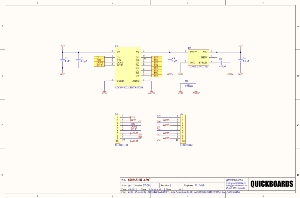
Precision Analog Supply and Reference Regulation
A major design choice in this block is the inclusion of U2, a TC1015-2.7V LDO regulator. While the ADC can run directly from the 3V3 digital rail, utilizing a dedicated 2.7V regulated supply for VA (Analog Supply) ensures a clean, stable full-scale reference voltage. In SAR ADCs, the analog supply often doubles as the reference; any ripple or noise on this rail translates directly into conversion errors or “jitter” in the digital output. By stepping down the 3V3 rail to 2.7V through a low-noise LDO, we isolate the conversion process from digital transients. C3 (1uF) provides bulk decoupling for this rail, while C5 (470pF) is connected to the LDO bypass pin to further reduce the internal reference noise floor of the regulator.
Mixed-Signal Grounding Strategy (Star Ground)
To maintain 10-bit accuracy, this design strictly separates AGND and DGND planes. Digital switching on the SCLK and DOUT lines creates high-frequency return currents that can interfere with the sensitive analog sampling process if shared on a single plane. These two grounds are bridged by R1, a 0 Ohm resistor, serving as a “net tie” or star-ground point. This ensures there is a single, unambiguous return path for the entire circuit while preventing digital noise from “polluting” the analog ground plane. Senior engineers will recognize this as a critical step in achieving the datasheet-specified Signal-to-Noise Ratio (SNR).
Digital Decoupling and Interface Filtering
The digital supply (VD) is powered by the 3V3 rail and filtered by a parallel combination of C1 (1uF) and C2 (0.1uF). Component selection here is deliberate: the 0.1uF ceramic capacitor is chosen for its low equivalent series resistance (ESR) and high self-resonant frequency, making it ideal for bypassing high-frequency logic noise. The 1uF capacitor acts as a local reservoir to stabilize the supply during the rapid current draws associated with the SAR bit-cycling process. These components must be placed within 2-3mm of Pin 13 to be effective.
Input Channel Routing and Connectors
The eight analog input channels are broken out via X1 and X2. To minimize crosstalk between adjacent channels during high-speed sampling, the AGND lines are interleaved where possible on the connectors. This provides a clear return path for each sensor signal and reduces the loop area, which is vital for EMI/EMC compliance in industrial applications.
Implementation Insights
When integrating this block into a larger system, the impedance of the analog source driving IN0-IN7 must be considered. SAR ADCs utilize an internal sampling capacitor that must be fully charged during the acquisition window. If the source impedance is too high (typically > 1k Ohm), the conversion result will be inaccurate. In such cases, an external operational amplifier should be used as a buffer for the input signals.
Common pitfalls include neglecting the trace width of the analog supply path. Even small parasitic resistances on the VA line can cause voltage drops that fluctuate with sampling speed, leading to non-linearity errors. Ensure that the trace from the U2 regulator output to Pin 2 is wide and as short as possible.
Applications
- Portable Instrumentation: Used for handheld data loggers and diagnostic tools requiring high precision and low battery drain.
- Industrial Process Control: Monitoring multiple 4-20mA or 0-5V sensor loops in factory automation.
- Medical Equipment: Interfacing with multi-lead electrode arrays for patient monitoring.
- Battery Management Systems: Precision monitoring of multi-cell battery packs for voltage balancing and health metrics.
Integrating the ADC108S022CIMTX into your design
This modular block provides a pre-validated data acquisition subsystem that eliminates the complexities of mixed-signal grounding and reference regulation. By utilizing the integrated TC1015 LDO and the net-tie grounding strategy, the design ensures that the 10-bit resolution is maintained even in noisy digital environments. This allows developers to focus on higher-level firmware and signal processing rather than fundamental analog hardware debugging.
Skip the tedious research and manual entry. Download the production-ready schematic block for the ADC108S022CIMTX directly from the Quickboards Library.