AD7689ACPZRL7 16bit Analog to Digital Converter Reference Schematic Design
The AD7689ACPZRL7 is a highly integrated, 8-channel, 16-bit, charge redistribution Successive-Approximation Register (SAR) Analog-to-Digital Converter. This IC is engineered for high-density, multichannel applications where precision and low power consumption are paramount. It includes an internal temperature sensor, a multi-channel multiplexer, and an internal reference, though it is often utilized with external stabilization as seen in this block. Typical applications include battery-powered instrumentation, medical diagnostic equipment, and multichannel system monitoring where 16-bit resolution provides the necessary dynamic range for low-level signal detection.
Unlock the Quickboards Library
Get instant access to this Altium Schematic and hundreds of other subcircuits. Hardware design, modularized. Schematic + Layout + Firmware. Built to IPC standards for zero re-spins.
Overview of the AD7689ACPZRL7
The device architecture is optimized for versatility, allowing the 8 analog inputs to be configured as single-ended, differential, or bipolar inputs relative to a common reference. The SAR architecture ensures zero latency and low power dissipation that scales directly with the sampling rate. This makes the AD7689 ideal for systems that cycle between high-activity sampling and low-power idle states.
| Technical Specification | Value |
| Resolution | 16-bit |
| Number of Channels | 8 (Multiplexed) |
| Architecture | SAR |
| Throughput | Up to 250 kSPS |
| Supply Voltage (VDD) | 2.3V to 5.5V |
| Interface | Serial SPI Compatible |
| SNR | 92 dB to 93 dB |
| Package | 20-lead LFCSP |
Pin Configuration and Function Mapping
The AD7689 utilizes a compact 20-lead footprint plus an exposed pad, facilitating high-density PCB layouts without compromising signal integrity.
| Pin Number | Primary Function | Secondary / Peripheral Functions |
| 1, 20 | VDD | Main Power Supply |
| 15 | VIO | Digital Interface Supply |
| 2 | VREF | Reference Input/Output |
| 3 | REFIN | Reference Buffer Input |
| 11 | CNV | Convert Input (Initiates Sampling) |
| 12 | DIN | Serial Data Input |
| 13 | SCK | Serial Clock Input |
| 14 | SDO | Serial Data Output |
| 4, 5, 21 | GND | Digital/System Ground (Includes EPAD) |
| 10 | COM | Common Analog Input Reference |
| 16 – 19 | IN0 – IN3 | Analog Input Channels 0-3 |
| 6 – 9 | IN4 – IN7 | Analog Input Channels 4-7 |
Functional Block Analysis & Design Decisions
Power and Decoupling Strategy
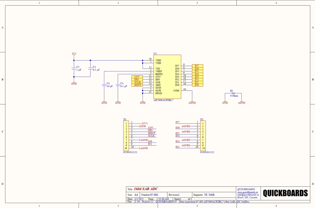
The power distribution network for this 16-bit converter is split between VDD (pins 1 and 20) and VIO (pin 15). Both are tied to the 3.3V rail in this implementation. Decoupling is achieved through a 1 microfarad bulk ceramic capacitor (C1) and a 0.1 microfarad high-frequency ceramic capacitor (C2). The 0.1 microfarad capacitor is selected for its low Equivalent Series Inductance (ESL) to filter high-frequency switching noise from the digital core and the logic interface. The 1 microfarad capacitor provides the necessary energy reservoir to handle the instantaneous current demands during the SAR bit-cycling process.
Reference Stabilization
A critical design choice in this block is the stabilization of the VREF and REFIN lines (pins 2 and 3). These pins are tied together and supported by a 10 microfarad (C3) and a 0.1 microfarad (C4) capacitor. In SAR converters, the internal capacitive DAC requires a large, low-impedance charge reservoir during the conversion phase to prevent voltage droop, which would otherwise manifest as gain errors or non-linearity. The 10 microfarad capacitor provides this reservoir, while the 0.1 microfarad capacitor ensures stability against high-speed transients.
Mixed-Signal Grounding and Net-Tying
To maintain 16-bit performance, the digital ground (GND) and analog ground (AGND) are isolated across the board but connected at a single star point via R1, a 0 Ohm resistor. This “net-tie” strategy ensures that high-speed digital return currents on the SPI bus do not flow through the sensitive analog return paths, which could introduce significant noise into the sampling COM line (pin 10). Pin 21 (EPAD) is tied to the digital ground plane to provide both electrical shielding and a thermal path for the IC.
Analog Front End and Interface
The 8 input channels are broken out to header X2, while the SPI interface is routed to header X1. The COM pin (pin 10) is tied directly to the AGND plane. This configuration assumes single-ended unipolar measurements. For differential configurations, the COM pin would be driven by a buffered reference. The SPI bus includes a conversion start signal (CNV), which is essential for precise control over the sampling window, minimizing aperture jitter in the system.
Implementation Insights
At 16-bit resolution, the reference voltage stability is the most frequent source of performance degradation. Engineers should ensure that the trace between the 10 microfarad capacitor (C3) and the VREF pin is as short and wide as possible to minimize parasitic resistance. Even a few milliohms of trace resistance can cause errors during the charge redistribution phase.
The VIO supply (pin 15) allows the ADC to interface with logic levels independent of the VDD supply. In this design, they are both 3.3V, but if the host microcontroller operates at 1.8V, VIO should be moved to that rail to avoid the need for external level shifters.
Significant design risks arise from improper soldering of the Exposed Pad (pin 21). In high-precision SAR converters, the EPAD serves as the primary ground reference for the internal substrate. If this pad is not securely bonded to the ground plane, the device may exhibit increased noise floors and erratic conversion results that are difficult to diagnose in software.
Applications
- Multichannel System Monitoring: The 8-channel multiplexer allows for sequential monitoring of various system voltages and sensors with a single converter.
- Battery-Powered Equipment: Ultra-low power consumption makes it ideal for handheld devices requiring long operational lifespans.
- Medical Instruments: Provides the high 16-bit resolution needed for low-frequency diagnostic signals such as those found in ECG or EEG equipment.
- Test and Measurement: High linearity and low noise make it suitable for benchtop and portable data acquisition systems.
Integrating the AD7689ACPZRL7 into your design
This modular block provides a pre-validated, layout-ready solution for 16-bit data acquisition. By adopting this schematic sub-system, engineers eliminate the risks associated with reference stabilization and mixed-signal grounding that often plague high-resolution converter designs. The inclusion of standardized headers and optimized decoupling ensures that the AD7689 can be dropped directly into any design, significantly reducing the hardware bring-up phase.
Skip the tedious research and manual entry. Download the production-ready schematic block for the AD7689ACPZRL7 directly from the Quickboards Library.