ATmega328P Reference Schematic Design
The ATmega328P is a high-performance, low-power Microchip 8-bit AVR RISC-based microcontroller. It has achieved industry-standard status as the core of the Arduino Uno, but its utility extends far beyond prototyping into production-ready industrial and consumer applications. Its architecture is designed to execute powerful instructions in a single clock cycle, enabling a throughput approaching 1 MIPS per MHz. This efficiency allow engineers to optimize power consumption while maintaining sufficient processing speed for tasks such as sensor interfacing, motor control, and complex logic execution.
Unlock the Quickboards Library
Get instant access to this Altium Schematic and hundreds of other subcircuits. Hardware design, modularized. Schematic + Layout + Firmware. Built to IPC standards for zero re-spins.
Overview of the ATmega328P
The ATmega328P is a versatile workhorse for embedded systems that require a balance of memory, I/O, and peripheral support in a cost-effective package. It is frequently utilized in battery-powered devices due to its picoPower technology, which minimizes power consumption in sleep modes.
| Feature | Specification |
| Core Architecture | 8-bit AVR RISC |
| Operating Voltage | 1.8V to 5.5V |
| Max Frequency | 20 MHz |
| Flash Memory | 32 KB |
| SRAM | 2 KB |
| EEPROM | 1 KB |
| ADC | 10-bit, 8-channel |
| Communication | UART, SPI, I2C |
| Package | 32-pin TQFP |
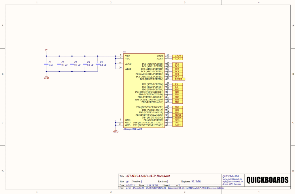
Pin Configuration and Function Mapping
The 32-pin TQFP package provides a dense layout that multiplexes digital I/O with specialized analog and communication functions.
| Pin Number | Primary Function | Secondary / Peripheral Functions |
| 4, 6 | VCC | Digital Supply Voltage |
| 18 | AVCC | Supply Voltage for ADC |
| 20 | AREF | Analog Reference Pin |
| 3, 5, 21 | GND | Ground Reference |
| 29 | PC6 | RESET / Interrupt |
| 30, 31 | PD0, PD1 | UART RX and TX |
| 7, 8 | PB6, PB7 | TOSC1, TOSC2 / Crystal Oscillator |
| 15, 16, 17 | PB3, PB4, PB5 | SPI MOSI, MISO, SCK |
| 23 – 28 | PC0 – PC5 | ADC Inputs / I2C SDA and SCL |
| 19, 22 | ADC6, ADC7 | Dedicated Analog Inputs |
Functional Block Analysis & Design Decisions
Power and Decoupling Strategy
The power block utilizes a multi-capacitor decoupling network to ensure rail stability across the 5V supply. A bulk 1uF ceramic capacitor (C1) handles low-frequency transients, while four 0.1uF capacitors (C2, C3, C4, C5) are strategically placed to filter high-frequency switching noise. For high-performance digital logic, 0.1uF X7R ceramic capacitors are the industry standard due to their low Equivalent Series Resistance (ESR) and stability over temperature. In physical layout, these capacitors must be placed as close as possible to the VCC/GND and AVCC/GND pin pairs. This minimizes the loop inductance of the power traces, preventing ground bounce and electromagnetic interference (EMI).
Timing and Oscillation
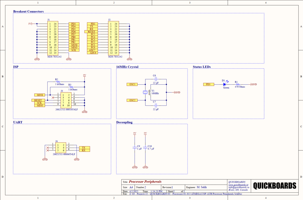
System timing is managed by a 16MHz crystal (Y1) paired with two 22pF C0G ceramic load capacitors (C6, C7). The selection of 22pF is calculated to match the crystal’s required load capacitance while accounting for stray PCB capacitance. Using C0G (NP0) dielectric capacitors is critical for the timing block because they maintain a consistent capacitance value despite temperature fluctuations, ensuring the system clock remains within the tolerances required for stable UART communication. Traces for the oscillator should be kept short and symmetrical to minimize parasitic effects.
In-System Programming (ISP)
The ISP block (J3) is broken out via a 10-pin header, providing a standardized interface for production programming. A 1kOhm resistor (R3) is implemented as a pull-up on the RESET line. This defines the default high state, preventing environmental noise from triggering a system reset. Another 1kOhm resistor (R2) is placed on the MOSI line; this acts as an isolation resistor to prevent signal contention between the programmer and other SPI peripherals on the board during the firmware upload process.
UART and Status Indication
Serial communication is routed through a 6-pin UART header (J4), enabling direct TX/RX interfacing with external telemetry or debugging tools. For visual diagnostics, a green status LED (D1) is connected to pin PD3. A 470 Ohm current-limiting resistor (R1) is used to set the LED current to approximately 7mA. This provides sufficient brightness for user feedback without placing an unnecessary thermal or current load on the microcontroller’s I/O port.
Implementation Insights
When integrating this ATmega328P block, engineers must ensure that AVCC is properly connected even if the ADC is not being used. Internal circuitry requires power on the AVCC pin for Port C to function correctly. In designs requiring high-precision analog measurements, the AVCC line should be filtered with a dedicated LC network (10uH inductor and 0.1uF capacitor) to isolate the analog block from digital switching noise.
Technical oversights to avoid include improper grounding of the crystal capacitors. These should be tied to a local ground plane that has a single-point connection to the main ground, reducing the risk of digital noise being injected into the clock circuit. Additionally, ensure the VCC rail is stable before the RESET line is released to prevent the MCU from entering an undefined state during power-up.
Applications
- IoT Sensor Nodes: Ideal for low-power data collection and transmission in wireless mesh networks.
- Industrial Logic Controllers: Used for managing relays, solenoids, and simple process automation where 8-bit precision is sufficient.
- Educational Development Boards: The standard platform for teaching embedded C and hardware-software interfacing.
- Handheld Consumer Electronics: Frequently manages user interfaces, battery monitoring, and peripheral control in portable devices.
Integrating the ATmega328P into your design
This modular block provides a pre-validated hardware foundation, ensuring that power integrity, timing, and programming interfaces are optimized for the ATmega328P. By utilizing this sub-system, you eliminate the repetitive task of configuring core support circuitry, allowing you to focus on application-specific logic and firmware development.
Skip the tedious research and manual entry. Download the production-ready schematic block for the ATmega328P directly from the Quickboards Library.