ATSAME70Q21B Reference Schematic Design
The ATSAME70Q21B is a high-performance 32-bit microcontroller based on the ARM Cortex-M7 processor core with a Floating Point Unit (FPU). Operating at speeds up to 300 MHz, this device represents the top tier of the SAM E series, engineered specifically for connectivity-intensive and high-computation embedded applications. It is frequently utilized in industrial automation gateways, high-speed communication hubs, and sophisticated consumer electronics that require a combination of Ethernet, dual CAN FD, and High-Speed USB. Its advanced architecture, featuring 2048 KB of Flash and 384 KB of multi-port SRAM, allows for deterministic real-time performance while managing complex communication stacks.
Unlock the Quickboards Library
Get instant access to this Altium Schematic and hundreds of other subcircuits. Hardware design, modularized. Schematic + Layout + Firmware. Built to IPC standards for zero re-spins.
Overview of the ATSAME70Q21B
The ATSAME70Q21B is designed to handle demanding workloads that exceed the capabilities of standard Cortex-M4 devices. It features a high-bandwidth internal bus matrix and dedicated DMA controllers to ensure data flows efficiently between peripherals and memory without taxing the CPU. Possible applications include automotive aftermarket control units, professional audio processing, and high-speed data acquisition systems.
| Feature | Specification |
| Core Architecture | 32-bit ARM Cortex-M7 |
| Maximum CPU Speed | 300 MHz |
| Flash Memory | 2048 KB |
| SRAM | 384 KB |
| Operating Voltage | 1.71V to 3.63V |
| Connectivity | Ethernet MAC, 2x CAN FD, USB HS |
| ADC | Dual 12-bit, 24-channel, 2 Msps |
| Timers | 12x 16-bit Timer/Counters |
| Package | 144-pin TQFP/LFBGA |
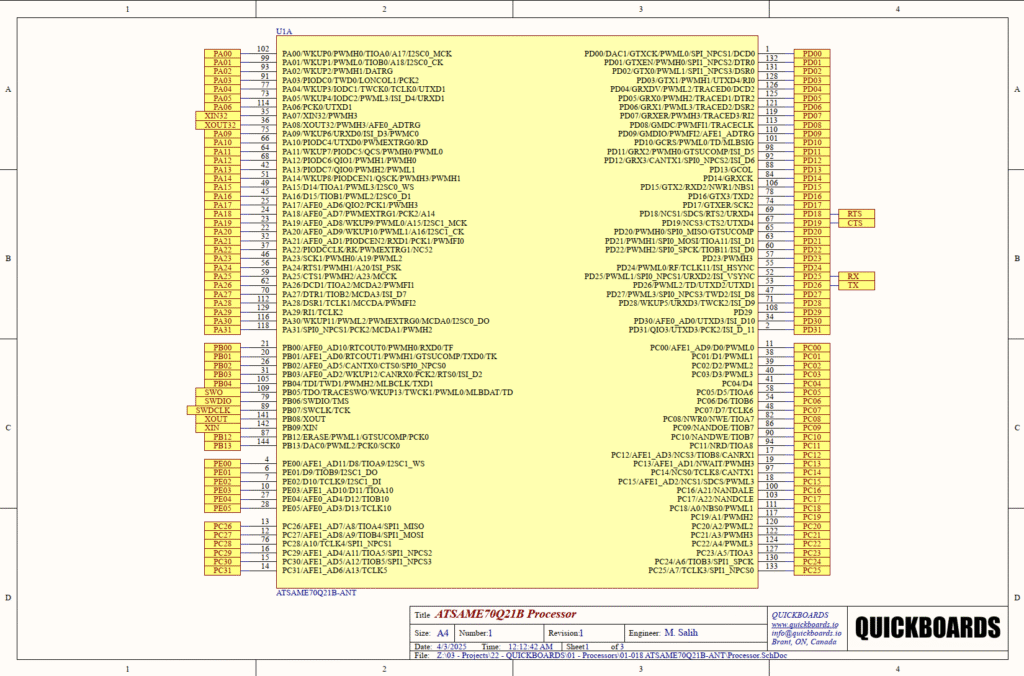
Pin Configuration and Function Mapping
The 144-pin configuration allows for a massive degree of peripheral concurrency, enabling high-speed communication and extensive analog interfacing without signal multiplexing conflicts.
| Pin Number | Primary Function | Secondary / Peripheral Functions |
| 134, 143 | VDDUTMII / VDDPLL | USB PHY and PLL Supply Rails |
| 3, 29, 33 | VDDOUT / VDDCORE | Internal LDO Output / Core Power |
| 102, 99 | PA00 / PA01 | PWMH0 / TIOA0 / UART0 |
| 89, 90 | SWDIO / SWDCLK | Serial Wire Debugging Interface |
| 141, 142 | XOUT / XIN | Main Crystal Oscillator (20 MHz) |
| 35, 36 | XOUT32 / XIN32 | RTC Crystal Oscillator (32.768 kHz) |
| 59, 67 | PD18 / PD19 | UART1 RTS / CTS Flow Control |
| 47, 71 | PD26 / PD27 | UART1 RX / TX Data |
| 5, 30, 43 | VDDIN / VDDIO | Main Power Input and I/O Rail |
| 11, 38, 39 | PC00 – PC02 | ADC Inputs / PWM Control |
Functional Block Analysis & Design Decisions
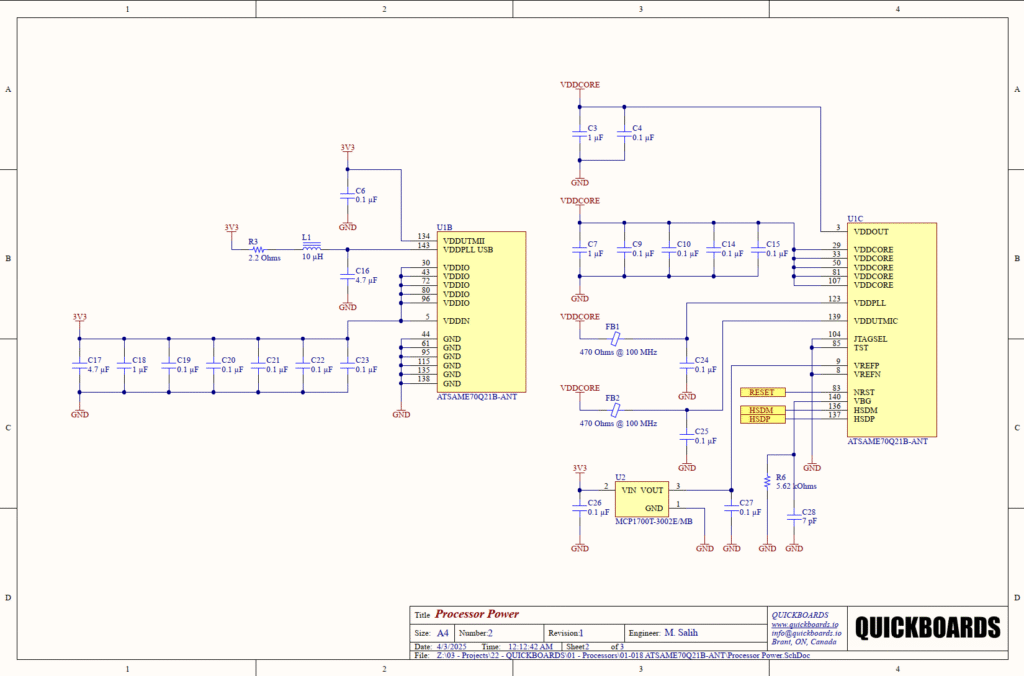
Processor Power and Core Regulation
The ATSAME70Q21B requires multiple voltage domains to maintain stability at 300 MHz. The design utilizes an MCP1700 series LDO to derive the VDDCORE rail (net 1.2V) from the main 3.3V input. This choice is based on the LDO’s low quiescent current and high stability, which is essential for the sensitive internal logic. The schematic employs a tiered decoupling strategy: VDDIN is filtered by a bulk 4.7uF ceramic capacitor (C17) and multiple 0.1uF/1uF local capacitors (C18-C23). For the VDDCORE domain, a high concentration of 0.1uF ceramic capacitors (C9, C10, C14, C15) is placed in parallel to minimize Equivalent Series Inductance (ESL), ensuring the core can draw rapid current spikes during high-frequency switching without voltage sagging.
Analog and PLL Noise Isolation
Sensitive analog and timing domains like VDDPLL, VDDUTMII, and VDDUTMIC require isolation from digital switching noise. The design implements a series of low-pass filters using 470 Ohm ferrite beads (FB1, FB2) and a 10uH inductor (L1) combined with 0.1uF capacitors. These filters suppress high-frequency electromagnetic interference (EMI) that could otherwise induce jitter in the PLL or degrade the signal-to-noise ratio of the USB PHY. The use of a 2.2 Ohm resistor (R3) in series with the USB power rail provides small-signal damping to prevent LC resonance in the power path.
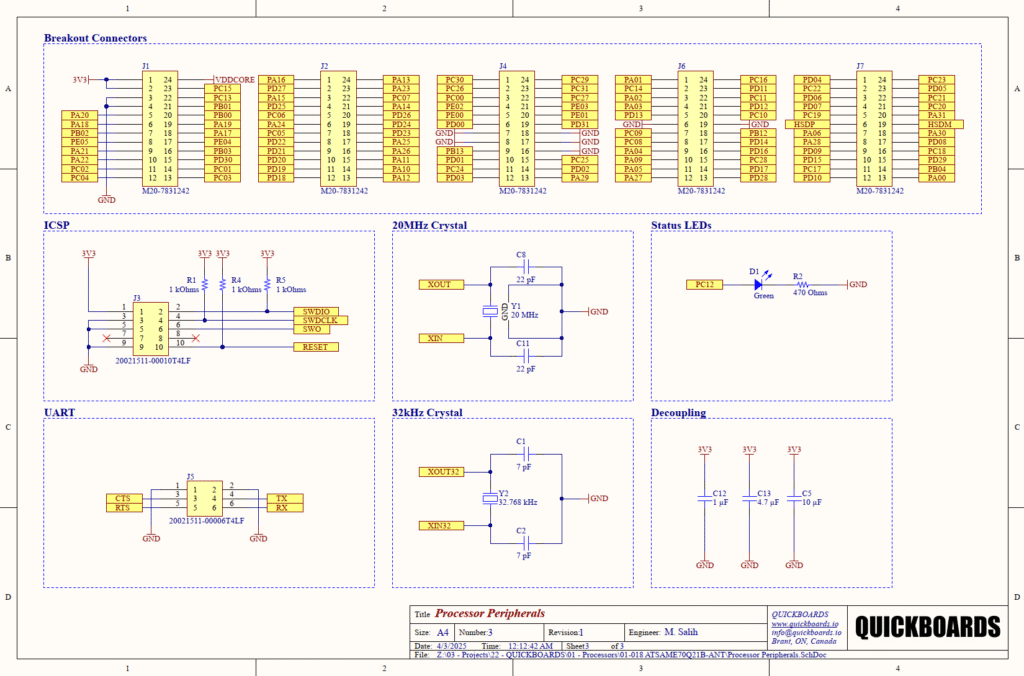
Timing and Oscillation
The timing block features two distinct crystal circuits. A 20 MHz crystal (Y1) with 22pF load capacitors provides the high-frequency reference for the internal PLLs. This specific frequency allows the system to reach its peak 300 MHz performance through internal multipliers. A secondary 32.768 kHz crystal (Y2) with 7pF load capacitors (C1, C2) is implemented for the Real-Time Clock (RTC) and low-power backup modes. The 7pF value is selected to match the high-impedance drive requirements of low-power watch crystals, ensuring reliable startup and long-term accuracy.
Programming and Debug Interface
A 10-pin header (J3) is used for the Serial Wire Debug (SWD) and JTAG interface. Pull-up resistors of 1kOhm (R1, R4, R5) are placed on the SWDIO, SWDCLK, and SWO lines. These values are lower than the typical 10kOhm to provide stronger noise immunity and sharper signal edges, which is critical when debugging at high interface speeds. The RESET line is similarly pulled high to VDDIO to prevent spurious system restarts in electrically noisy industrial environments.
Status and Connectivity
Visual feedback is provided via a green status LED (D1) connected to PC12 through a 470 Ohm current-limiting resistor (R2). This provides approximately 3.5mA, ensuring visibility without excessive power consumption. The main I/O ports are broken out through high-density M20 series connectors (J1, J2, J4, J6, J7), allowing this processor block to interface with high-speed memory extensions or custom interface boards while maintaining signal integrity across the interconnection.
Implementation Insights
When integrating the ATSAME70Q21B, the layout of the VDDCORE decoupling capacitors is paramount. These must be placed as close to the BGA/TQFP power pins as possible, ideally using a via-in-pad or near-pad strategy to reduce the total loop inductance. At 300 MHz, even a few millimeters of trace can introduce enough impedance to cause logic errors during peak execution cycles.
Grounding strategy for the analog section (VREFP/VREFN) should involve a dedicated analog ground plane or a quiet “island” tied to the main digital ground at a single star point. This prevents return currents from the high-speed digital bus matrix from interfering with the 12-bit ADC results.
Applications
- Industrial Ethernet Gateways: High-speed processing allows for real-time protocol conversion between Ethernet/IP, CAN FD, and legacy serial interfaces.
- Professional Audio Equipment: The Cortex-M7 FPU and high-speed memory facilitate real-time digital signal processing (DSP) for audio mixing and effects.
- Advanced Motor Control: Integrated high-resolution PWMs and dual ADCs enable Field Oriented Control (FOC) for multi-axis robotic systems.
- Human Machine Interfaces (HMI): Sufficient SRAM and clock speed to drive medium-resolution graphical displays and touch interfaces in industrial panels.
Integrating the ATSAME70Q21B into your design
This modular reference block provides a pre-validated, production-ready solution for the core support circuitry required by the ATSAME70Q21B. By adopting this schematic sub-system, engineers eliminate the risks associated with core power sequencing, PLL noise filtering, and high-frequency clocking layout. The inclusion of standardized breakout connectors and robust programming interfaces ensures that the hardware bring-up process is streamlined, allowing the design team to focus on application-layer firmware and system-level integration.
Skip the tedious research and manual entry. Download the production-ready schematic block for the ATSAME70Q21B directly from the Quickboards Library.