VL53L5CXV0GC/1 Multizone Optical Distance Sensor Reference Schematic Design
The VL53L5CXV0GC/1 is a state-of-the-art, multizone Time-of-Flight (ToF) ranging sensor from STMicroelectronics. Unlike standard single-point distance sensors, this device utilizes an advanced metasurface lens architecture to provide a wide 63-degree diagonal field of view, capable of outputting ranging data for up to 8×8 (64) discrete zones. Its primary function is to provide high-speed, accurate distance mapping, making it essential for complex spatial awareness tasks. Typical applications include gesture recognition, floor mapping for vacuum robots, occupancy sensing in smart buildings, and laser-assisted autofocus for high-end camera systems.
Overview of the VL53L5CXV0GC/1
The sensor integrates a 940nm Vertical-Cavity Surface-Emitting Laser (VCSEL) and a SPAD (Single Photon Avalanche Diode) detector array. By measuring the “time of flight” of individual photons, it calculates distance regardless of target color or reflectivity. The VL53L5CXV0GC/1 is designed to operate in high-ambient light conditions and provides autonomous ranging with programmable interrupt thresholds for each zone, significantly reducing the host processor’s workload.
| Technical Specification | Value |
| Supply Voltage (AVDD/IOVDD) | 2.8V to 3.3V |
| Range | 2 cm to 400 cm |
| Multizone Configuration | 4×4 or 8×8 zones |
| Field of View (FoV) | 63 degrees Diagonal |
| Max Frame Rate | 60 Hz |
| Communication Interface | I2C (up to 1 MHz) or SPI |
| Laser Wavelength | 940 nm (Class 1) |
| Operating Temperature | -30 to 85 degrees Celsius |
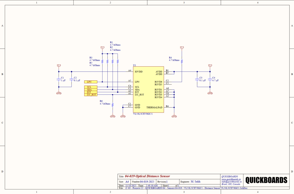
Pin Configuration and Function Mapping
The VL53L5CXV0GC/1 utilizes a specialized optical LGA package. The mapping below reflects the specific configuration used in this reference block to support I2C communication and interrupt-driven operation.
| Pin Number | Primary Function | Secondary / Peripheral Functions |
| A1 | I2C_RST | Hardware reset for I2C bus |
| A3 | INT | Programmable Interrupt Output |
| A4 | IOVDD | I/O and Digital Power Supply |
| A5 | LPN | Low Power Now (Active Low) |
| B1, B7 | AVDD | Analog and Laser Power Supply |
| B4 | THERMALPAD | System Ground / Heat Dissipation |
| C3 | SDA | I2C Serial Data |
| C4 | SCL | I2C Serial Clock |
| C1, C7 | GND | System Ground |
| C2, C5 | RSVD6, RSVD5 | Internal Logic Reference (Must be pulled high) |
| A2, A6, A7, C6 | RSVD4, RSVD1, RSVD2, RSVD3 | Reserved Ground Terminals |
Functional Block Analysis & Design Decisions
Power and Decoupling Block
The schematic implements a dual-rail power strategy separating the analog/laser supply (AVDD) from the digital I/O supply (IOVDD). To ensure stable ranging, AVDD is decoupled by C3 (0.1 uF) and C4 (4.7 uF). The 4.7 uF capacitor is a critical choice; it provides the localized bulk energy required for the high-peak current pulses of the 940nm VCSEL. IOVDD uses C1 (1 uF) and C2 (0.1 uF) to filter high-frequency switching noise from the digital logic. Ceramic X7R capacitors are specified here for their low Equivalent Series Resistance (ESR) and stability across temperature, which prevents voltage droop during laser emission.
Digital Control and Interface Block
The communication block is configured for Fast-mode Plus I2C (up to 1 MHz). Resistors R1 and R2 (4.7 kOhms) provide the necessary pull-up for the I2C bus. The LPN (Low Power Now) pin is pulled high by R3 (4.7 kOhms) to keep the sensor active by default, while the INT pin uses R5 (4.7 kOhms) as a pull-up to support the open-drain interrupt architecture. A notable design choice is R6, a 4.7 kOhm pull-down on the I2C_RST pin. This ensures the sensor is not inadvertently held in reset during power-up, providing a deterministic startup sequence.
RSVD Pin Termination
Senior engineers will note the treatment of the Reserved (RSVD) pins. Pins C2 and C5 are tied to 3.3V via R4 (4.7 kOhms). This is a manufacturer-specific requirement to bias internal logic correctly. Pins A2, A6, A7, and C6 are tied directly to the ground plane. This configuration maximizes the shielding of the sensitive SPAD array from electromagnetic interference and improves the thermal path from the silicon to the PCB ground plane.
Implementation Insights
A primary engineering consideration for the VL53L5CXV0GC/1 is the optical keep-out zone. Since this is a wide-FoV multizone sensor, any mechanical obstruction or cover glass placed too close to the emitter or receiver will cause “internal crosstalk.” This manifests as a false signal where the sensor ranges its own cover glass rather than the target. If a cover glass is used, it must be an optical-grade material with a low refractive index and high 940nm transmission.
Integration of this block also requires significant firmware overhead. Unlike simpler sensors, the VL53L5CXV0GC/1 requires a Large Driver (ULD) to manage the multizone data processing. Designers must ensure the host microcontroller has at least 80 KB of Flash and sufficient RAM to handle the data buffers generated by the 8×8 zone configuration.
Thermal management is vital for maintaining ranging accuracy. The B4 Thermal Pad must be soldered to a significant ground pour. Excessive heat at the sensor junction can cause wavelength shifts in the VCSEL, leading to ranging errors or reduced sensitivity in the SPAD array.
Applications
- Robotics and Drones: Provides real-time obstacle detection and floor cliff sensing with wide-angle coverage.
- Gestural Control: Enables touchless interfaces by tracking hand position and movement across multiple zones.
- Occupancy Sensing: Accurately counts people entering or leaving a room by detecting direction of movement through the multizone grid.
- Liquid Level Sensing: Monitors fluid levels in containers where the surface may be agitated, using multizone averaging to improve reliability.
Integrating the VL53L5CXV0GC/1 into your design
This modular block provides a production-ready implementation of a multizone spatial sensor, eliminating the complexity of laser supply decoupling and reserved pin biasing. By providing pre-validated pull-up and pull-down configurations for the digital control lines, the design reduces the risk of I2C bus lockups or initialization failures. This reusable sub-system allows teams to bypass the fundamental physics of ToF integration and focus on high-level spatial mapping algorithms.
Skip the tedious research and manual entry. Download the production-ready schematic block for the VL53L5CXV0GC/1 directly from the Quickboards Library.