RN4870-V/RM140 Bluetooth Low Energy (BLE) Reference Schematic Design
The RN4870-V/RM140 is a complete, fully certified Bluetooth Low Energy (BLE) 5.0 module designed for simple integration into embedded systems. Developed by Microchip, it utilizes a transparent UART-based ASCII command interface, allowing developers to implement wireless connectivity without the need for deep Bluetooth stack knowledge. This module is typically found in IoT sensor nodes, medical monitoring equipment, and industrial data loggers where low power consumption and rapid time-to-market are primary requirements.
Overview of the RN4870-V/RM140
As a surface-mount module, the RN4870 integrates a Bluetooth stack, onboard antenna, and radio frequency (RF) circuitry into a compact footprint. It supports the latest BLE 5.0 standards, including secure pairing and data streaming. By acting as a wireless replacement for serial cables, it enables smartphones or tablets to act as human-machine interfaces (HMI) for legacy industrial hardware.
| Feature | Specification |
| Bluetooth Standard | Bluetooth 5.0 Low Energy |
| Operating Voltage | 1.9V to 3.6V |
| TX Power | +2 dBm |
| RX Sensitivity | -90 dBm |
| Communication Interface | UART (Transparent/Command Mode) |
| Onboard Peripherals | SPI, I2C, PWM, 10-bit ADC |
| Security | 128-bit AES Encryption |
| Certification | FCC, IC, CE, QDID, KCC |
Pin Configuration and Function Mapping
The RN4870 provides a high degree of flexibility by multiplexing communication protocols and general-purpose I/O (GPIO) across its pinout.
| Pin Number | Primary Function | Secondary / Peripheral Functions |
| 4 | VBAT | Main Power Supply Input |
| 21 | RST_N | System Reset (Active-Low) |
| 23 | UART_TX | Serial Data Transmit |
| 22 | UART_RX | Serial Data Receive |
| 17 | P3_6 / RTS | UART Request to Send / GPIO |
| 15 | P0_0 / CTS | UART Clear to Send / GPIO |
| 27 | SCLK | SPI Clock / I2C Clock |
| 26 | MOSI | SPI Master Out Slave In / I2C SDA |
| 25 | MISO | SPI Master In Slave Out |
| 24 | CS | SPI Chip Select |
| 1, 2, 3, 31-33 | GND | System Ground |
Functional Block Analysis & Design Decisions
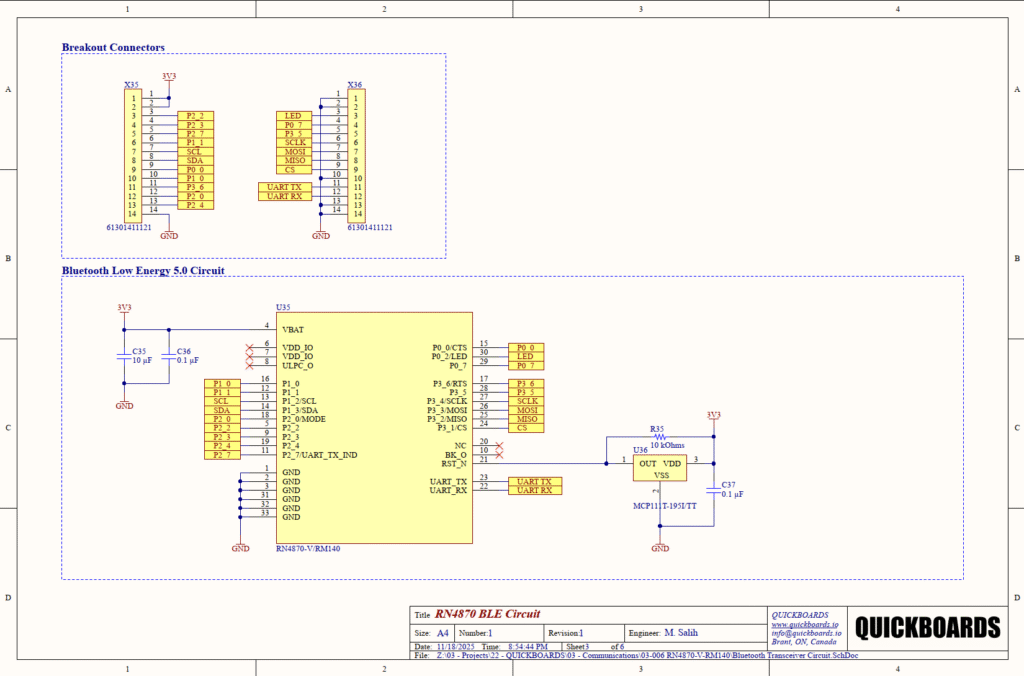
Power and Decoupling Strategy
The power sub-circuit for the RN4870 is designed to handle the transient current spikes common in RF transmission. The 3.3V rail is filtered by C35 (10uF) and C36 (0.1uF) ceramic capacitors. The 10uF capacitor serves as a bulk energy reservoir to minimize voltage sag during high-power radio states, while the 0.1uF capacitor provides high-frequency decoupling. For RF modules, X7R dielectric ceramic capacitors are preferred over electrolytic types due to their lower equivalent series resistance (ESR) and superior stability over temperature. These components must be placed as close as possible to the VBAT pin (Pin 4) to minimize trace inductance, which can lead to unpredictable RF performance or system resets.
System Reset and Voltage Supervision
Reliability in the field is enhanced by the inclusion of U36, an MCP111T-195I/TT voltage supervisor. This IC monitors the system voltage and ensures the BLE module remains in a reset state until the power rail is stable. The RST_N pin (Pin 21) is held low by the supervisor during power-up or brown-out conditions. R35 (10kOhms) acts as a standard pull-up resistor to the 3.3V rail, defining the default “not reset” state once the supervisor releases the line. Using a dedicated supervisor rather than a simple RC delay circuit prevents the module from entering an undefined state during slow power-on ramps, a critical choice for professional-grade hardware.
Communication and Signal Conditioning
The module is interfaced via two 14-pin breakout connectors (X35, X36), which facilitate easy integration with a host microcontroller. The UART interface includes hardware flow control (RTS/CTS), which is highly recommended for BLE applications. Because wireless data rates can vary based on signal strength and congestion, hardware flow control prevents serial buffer overflows in the module’s firmware. The SPI and I2C lines are also broken out to allow the module to act as a master controller for external sensors in standalone “Scripting Mode” applications.
Implementation Insights
When integrating the RN4870 block, the most critical physical layout requirement is the antenna keep-out area. To ensure maximum wireless range and signal integrity, the area directly beneath and around the ceramic chip antenna must be free of copper planes, traces, and metallic enclosures. Placing the module at the edge of the PCB is standard practice to allow the RF energy to radiate efficiently into free space.
Host microcontrollers must be configured to use a default baud rate of 115,200 bps when first communicating with the module. During the integration phase, ensuring the RST_N line is not floating is vital; while the onboard supervisor handles power-on reset, any external logic controlling this pin should be checked for high-impedance states that could lead to intermittent connectivity.
Applications
- Medical and Health Devices: Enables wireless data logging for heart rate monitors or glucose meters while maintaining strict battery life constraints.
- IoT Sensor Nodes: Functions as a gateway for smart home sensors, providing an easy path for environmental data to reach mobile applications.
- Industrial Automation: Replaces wired RS-232/RS-485 interfaces with a secure BLE link for configuration and diagnostics of factory equipment.
- Human Interface Devices (HID): Serves as the wireless backbone for custom keyboards, mice, or specialized game controllers.
Integrating the RN4870-V/RM140 into your design
This modular block provides a pre-validated, certified foundation for adding wireless connectivity to any project. By using this schematic sub-system, engineers eliminate the complexity of RF impedance matching and the risks associated with power-on reset instability. The design is structured to allow the module to operate either as a serial bridge or a standalone controller, significantly reducing development cycles and testing costs.
Skip the tedious research and manual entry. Download the production-ready schematic block for the RN4870-V/RM140 directly from the Quickboards Library.