PIC32MX795F512LT Reference Schematic Design
The PIC32MX795F512LT represents the pinnacle of Microchip’s MIPS32 M4K-based microcontroller lineup. This high-performance 32-bit MCU is engineered for connectivity-intensive applications, featuring integrated Ethernet MAC, Full-Speed USB 2.0 OTG, and dual CAN 2.0B controllers. It is a preferred choice for engineers developing industrial gateways, high-end audio processing systems, and complex embedded networking nodes that require significant memory overhead and fast execution speeds.
Overview of the PIC32MX795F512LT
Equipped with 512 KB of Flash and 128 KB of RAM, the PIC32MX795F512LT provides the resources necessary to run RTOS-based applications and extensive communication stacks simultaneously. Its architecture supports 80 MHz operation, delivering 105 DMIPS performance, while maintaining a flexible peripheral set that includes a 10-bit ADC, multiple serial interfaces, and a Parallel Master Port (PMP).
| Feature | Specification |
| Core Architecture | 32-bit MIPS32 M4K |
| Max CPU Speed | 80 MHz |
| Operating Voltage | 2.3V to 3.6V |
| Program Memory | 512 KB Flash |
| RAM | 128 KB |
| Ethernet | 10/100 Base-TX MAC |
| USB | 2.0 OTG Full-Speed |
| CAN | 2x CAN 2.0B Modules |
| ADC | 10-bit, 1 Msps, 16-ch |
| Package | 100-pin TQFP |
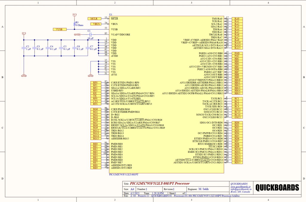
Pin Configuration and Function Mapping
The 100-pin TQFP package provides a vast array of multiplexed pins. The mapping below identifies key pins utilized in this reference block for power, timing, and communication.
| Pin Number | Primary Function | Secondary / Peripheral Functions |
| 13 | MCLR | Master Clear / Programming Voltage |
| 54, 55 | VBUS / VUSB | USB Power and Internal Regulator |
| 85 | VCAP/VDDCORE | Core Voltage Filter (Internal Regulator) |
| 2, 16, 37, 46, 62, 86 | VDD | Digital Logic Power (3.3V) |
| 30, 31 | AVDD / AVSS | Analog Power and Ground Reference |
| 63, 64 | OSC1 / OSC2 | Main System Oscillator Inputs |
| 24, 25 | PGEC1 / PGED1 | ICSP Clock and Data |
| 51, 50 | U1RX / U1TX | UART1 Receive and Transmit |
| 49, 40 | RTS / CTS | UART1 Hardware Flow Control |
| 6, 73, 74, 95 | SOSC / TCLK | Secondary Osc / Timer Inputs |
Functional Block Analysis & Design Decisions
Power and Decoupling Strategy
The PIC32MX architecture requires a robust power distribution network to handle high-frequency switching transients across its digital core. The design utilizes a bulk 1uF ceramic capacitor (C2) paired with five 0.1uF ceramic capacitors (C3, C4, C5, C6, C7) distributed across the VDD pins. These 0.1uF capacitors must be placed in immediate proximity to each VDD/VSS pin pair to minimize parasitic inductance. A specialized decoupling block (C12, C13) with 1uF and 4.7uF values provides additional filtering for the 3.3V rail. For the internal core regulator, a 10uF capacitor (C1) is connected to the VCAP pin. This is a non-polarized ceramic capacitor with low ESR (typically under 1 Ohm), which is mandatory for the stability of the 1.8V internal logic rail.
Timing and Oscillation
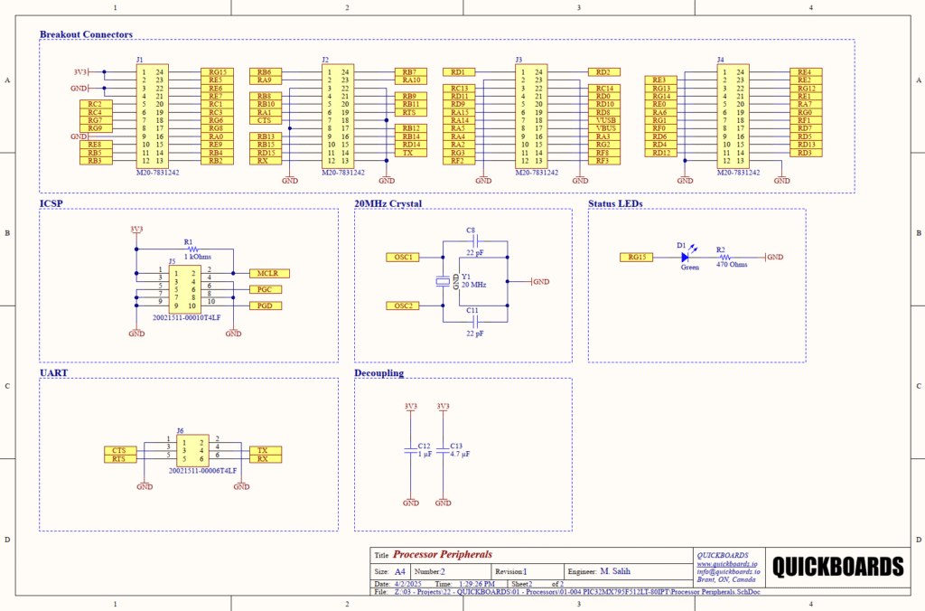
System timing is driven by a 20MHz crystal (Y1) with two 22pF C0G ceramic load capacitors (C8, C11). This frequency is ideal for the PIC32MX, as the internal Phase-Locked Loop (PLL) can multiply this reference to reach the maximum 80MHz operating frequency while simultaneously providing the 48MHz clock required for USB operations. The ground connection for the load capacitors is tied to a local “quiet” ground island to prevent digital noise from inducing jitter into the clock signal.
In-Circuit Serial Programming (ICSP)
The programming interface (J5) follows the standard Microchip 10-pin footprint. A 1kOhm pull-up resistor (R1) is connected to the MCLR pin. This ensures the device remains out of reset during normal operation while providing a current-limited path for the programmer to drive the line. The PGC and PGD lines are kept free of heavy capacitive loads to maintain the signal integrity required for high-speed debugging via tools like the MPLAB ICD or Real ICE.
USB and UART Interfaces
The UART block (J6) is configured with CTS and RTS pins, which is essential for high-speed 32-bit applications where the processor may be handling heavy Ethernet or USB traffic. Hardware flow control prevents data loss during these intensive CPU cycles. On the power side, a 0 Ohm resistor (R3) bridges the VUSB and 3.3V rails, allowing the internal USB transceiver to be powered by the system rail.
Status Indication and I/O Breakout
Status monitoring is provided by a green LED (D1) on pin RG15, limited by a 470 Ohm resistor (R2). This allows for visual heartbeat or error code signaling without significant power overhead. The design also breaks out the extensive I/O count through four 24-pin M20 connectors (J1-J4), providing access to the Ethernet, CAN, and PMP pins for modular expansion.
Implementation Insights
When integrating the PIC32MX795, layout engineers must prioritize the VCAP capacitor placement. Since the internal core logic operates at a lower voltage, any instability in this regulator can lead to “hard faults” or code execution errors that are difficult to debug in software.
Another consideration is the analog supply. AVDD and AVSS should be fed through a ferrite bead if the 10-bit ADC is being used for high-precision measurements. While this schematic provides a direct 3.3V connection for general-purpose use, adding local LC filtering is standard practice for senior-level designs requiring high Signal-to-Noise Ratio (SNR).
Applications
- Web Servers and Network Gateways: Utilizes the onboard Ethernet MAC to provide high-speed connectivity for IoT infrastructure.
- Digital Audio Processing: High CPU MIPS and large RAM allow for real-time filtering and decoding of digital audio streams.
- Industrial CAN Networks: Dual CAN controllers enable the device to act as a bridge or master node in automotive or factory automation environments.
- USB Host/Device Controllers: Integrated OTG support allows for interfacing with thumb drives, keyboards, or acting as a custom peripheral for a PC.
Integrating the PIC32MX795F512LT into your design
Implementing a 100-pin 32-bit MCU requires significant attention to power integrity and clocking. This modular block provides a pre-vetted foundation, ensuring that the critical core regulator, programming interfaces, and high-speed clocking circuits are implemented according to industry standards. By utilizing this sub-system, you reduce the risk of power-related resets and timing errors in the first spin of your PCB.
Skip the tedious research and manual entry. Download the production-ready schematic block for the PIC32MX795F512LT directly from the Quickboards Library.