MCP601T-I/OT 6 Channel Multiple Feedback High Pass Filter Reference Schematic Design
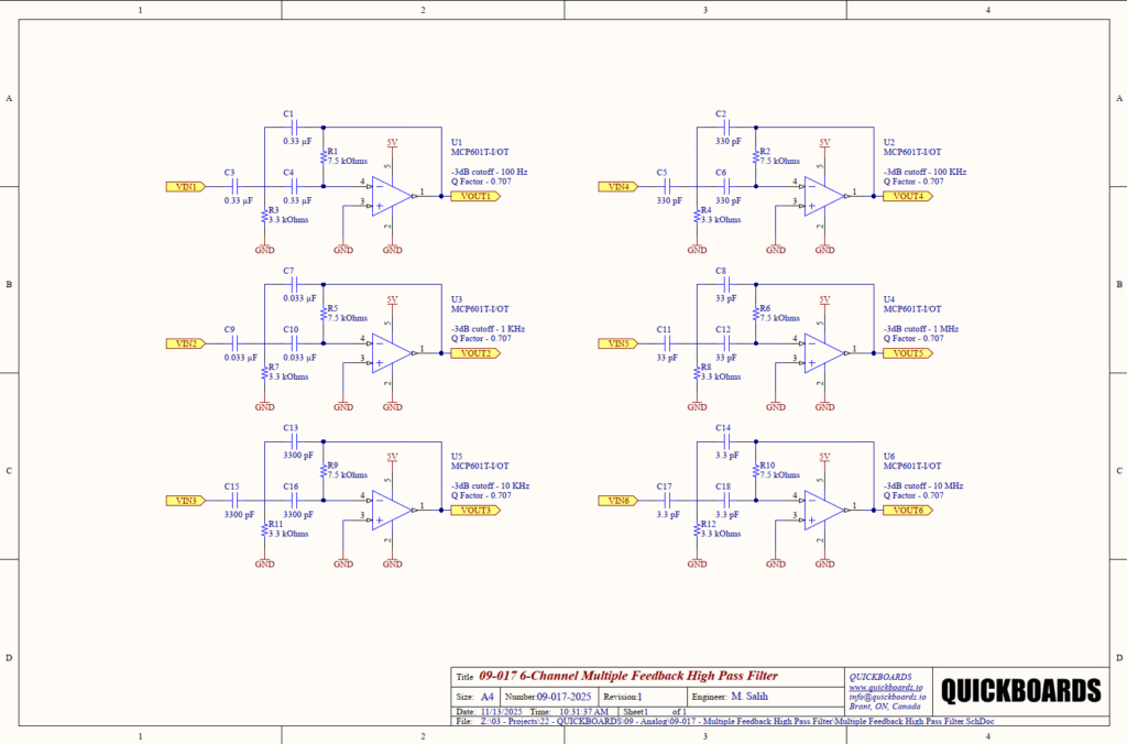
The MCP601T-I/OT is a low-power, rail-to-rail output operational amplifier designed by Microchip Technology. It is a cornerstone for precision signal conditioning in battery-powered and industrial environments, operating with a single supply voltage as low as 2.7V. In this reference schematic, the IC is utilized as the active element in a 6-channel Multiple Feedback (MFB) high-pass filter array. This topology is primarily used to remove DC offsets, low-frequency rumble, or 50/60 Hz mains interference from sensitive sensor data while providing a robust, low-impedance output for downstream digitization.
Overview of the MCP601T-I/OT
As a CMOS-based amplifier, the MCP601 provides extremely low input bias currents, which is essential for active filter designs using high-value resistors. Its 2.8 MHz Gain Bandwidth Product (GBWP) allows it to handle audio-band and low-frequency ultrasonic signals with high fidelity. The device is particularly suited for applications such as automotive sensor interfaces, portable medical instrumentation, and industrial process control where space and power efficiency are primary constraints.
| Technical Specification | Value |
| Supply Voltage Range | 2.7V to 6.0V |
| Gain Bandwidth Product | 2.8 MHz |
| Slew Rate | 2.3 V/us |
| Quiescent Current | 230 uA typical |
| Input Offset Voltage | 2 mV maximum |
| Output Type | Rail-to-Rail |
| Phase Margin | 50 degrees |
| Package | 5-lead SOT-23 |
Pin Configuration and Function Mapping
The MCP601T-I/OT is housed in a compact SOT-23 package, allowing for dense multi-channel filter implementations.
| Pin Number | Primary Function | Secondary / Peripheral Functions |
| 1 | VOUT | Amplifier Output / Feedback Node |
| 2 | VSS | Negative Supply / Ground Reference |
| 3 | VIN+ | Non-inverting Input (Reference GND) |
| 4 | VIN- | Inverting Input (Filter Summing Node) |
| 5 | VDD | Positive Supply (5V) |
Functional Block Analysis & Design Decisions
Active Signal Conditioning (Multiple Feedback High Pass Filter)
The primary functional block in this schematic is a 2nd order active Multiple Feedback (MFB) high-pass filter. This topology is selected for its superior stability and better stop-band rejection compared to the Sallen-Key configuration. In this design, the non-inverting input (Pin 3) is tied to ground, creating an inverting filter stage. Each channel is tuned to a Q-factor of 0.707, achieving a Butterworth response. This response is critical for engineering applications requiring a maximally flat passband, ensuring that the signals of interest are not distorted by peaking before the roll-off occurs.
Technical Deep-Dive: Frequency Scaling and BOM Standardization
The design covers a wide frequency spectrum from 100 Hz to 10 MHz across six independent channels. To optimize the Bill of Materials (BOM), the resistance values are standardized at R1=7.5 kOhms and R3=3.3 kOhms across all channels. Senior engineers will recognize that keeping resistance values constant while scaling capacitors by powers of 10 simplifies procurement and assembly without sacrificing performance. The 3.3 kOhm and 7.5 kOhm values are chosen to keep thermal noise floors minimal while remaining well within the drive capabilities of the MCP601 output stage.
Component Selection: Stability and Dielectrics
The selection of capacitors is frequency-dependent. For lower frequency channels (100 Hz to 10 kHz), ceramic X7R capacitors are used for their high volumetric efficiency. However, for the high-frequency channels (100 kHz to 10 MHz), C0G (NP0) dielectrics are mandatory. C0G capacitors provide a near-zero temperature coefficient and negligible voltage coefficient, ensuring the filter pole does not shift as the signal amplitude or ambient temperature fluctuates. Values scale from 0.33 uF for the 100 Hz cutoff down to 3.3 pF for the 10 MHz cutoff.
Placement and Trace Logic
Physical layout for high-pass filters requires the feedback loop capacitors to be placed as close to the IC pins as possible. Specifically, C1 (and its equivalents in other channels) must be positioned near Pin 1 and Pin 4 to minimize the trace area of the sensitive high-impedance inverting node. This reduces susceptibility to electromagnetic interference (EMI). A solid ground plane is essential for the shunt resistors (R3, R7, etc.) to provide a low-impedance return path, preventing ground-loop noise from modulating the filter’s baseline.
Design Rationale: DC Blocking and Phase Inversion
The input capacitors (e.g., C3 and C4) serve a dual purpose: they define the filter poles and act as high-quality DC blocks. In high-pass applications, this prevents DC offsets from the input source from saturating the amplifier rails. Because this is an MFB topology, the output signal is inverted 180 degrees relative to the input. Senior designers must account for this phase inversion in the downstream signal processing or software algorithms.
Implementation Insights
When integrating the MCP601T-I/OT into a larger system, the Gain Bandwidth Product (GBWP) remains the primary constraint. While the schematic includes a 10 MHz channel (U6), the 2.8 MHz GBWP of the MCP601 means that the active filtering performance will degrade significantly at this frequency. For the 1 MHz and 10 MHz channels, the op-amp acts more as a low-impedance buffer than a precise active filter stage. For applications requiring sharp active roll-offs above 1 MHz, a higher-speed amplifier from the Quickboards library would be more appropriate.
Digital noise from nearby microcontrollers can couple into the high-impedance feedback loops of the MFB topology. It is advisable to use a dedicated analog ground plane and keep digital traces away from the VIN- summing node. Additionally, although not explicitly shown in every sub-block, 0.1 uF ceramic decoupling capacitors must be placed within 2 mm of the VDD pin (Pin 5) for every IC to ensure high-frequency stability.
Applications
- Sensor Baseline Restoration: Removing slow-moving DC drift and 50/60 Hz hum from industrial pressure and temperature sensors.
- Audio Signal Processing: Eliminating sub-sonic rumble and DC offsets in microphone pre-amplifiers and line-level interfaces.
- Medical Diagnostic Equipment: Removing large DC offsets from biopotential electrodes (ECG/EEG) while preserving high-frequency biological data.
- Vibration Analysis: Filtering out low-frequency mechanical noise in accelerometer-based condition monitoring systems.
Integrating the MCP601T-I/OT into your design
The 09-017 6-Channel Multiple Feedback High Pass Filter block provides a production-ready, modular solution for multi-decade frequency management. By utilizing the MCP601’s rail-to-rail capabilities and standardized resistor networks, this block eliminates the repetitive iterative calculations usually required for high-order filter design. It offers a stable, low-impedance output that is ready to interface with any modern high-speed data acquisition system.
Skip the tedious research and manual entry. Download the production-ready schematic block for the MCP601T-I/OT directly from the Quickboards Library.