MCP601T-I/OT 6 Channel Multiple Feedback Low Pass Filter Reference Schematic Design
The MCP601T-I/OT is a low-power, CMOS operational amplifier featuring a 2.8 MHz Gain Bandwidth Product (GBWP) and rail-to-rail output swing. Designed by Microchip Technology, this integrated circuit is optimized for single-supply operation, making it a staple in portable instrumentation, sensor signal conditioning, and battery-powered applications. Its primary function in this reference design is to act as the active element in a 2nd-order Multiple Feedback (MFB) low pass filter, providing precise frequency discrimination with high stability.
Typical applications for this device include automotive sensor interfaces, industrial process control, and medical instrumentation where low quiescent current (230 microamps typical) and low input bias current are required to maintain signal integrity over high-impedance sources.
| Technical Specification | Details |
| Gain Bandwidth Product | 2.8 MHz |
| Operating Voltage Range | 2.7V to 6.0V |
| Input Offset Voltage | 2 mV (Maximum) |
| Input Bias Current | 1 pA (Typical) |
| Slew Rate | 2.3 V/microsecond |
| Output Swing | Rail-to-Rail |
| Quiescent Current | 230 microamps (Typical) |
| Package | 5-Lead SOT-23 |
Pin Configuration and Function Mapping
The MCP601T-I/OT is utilized in a compact SOT-23-5 package, providing a streamlined footprint for multi-channel filter arrays.
| Pin Number | Primary Function | Secondary / Peripheral Functions |
| 1 | VOUT | Analog Output / Feedback Node |
| 2 | VSS | Negative Power Supply / Ground |
| 3 | VIN+ | Non-Inverting Input |
| 4 | VIN- | Inverting Input / Summing Node |
| 5 | VDD | Positive Power Supply (e.g., 5V) |
Functional Block Analysis & Design Decisions
Active Filter Stage (Multiple Feedback Topology)
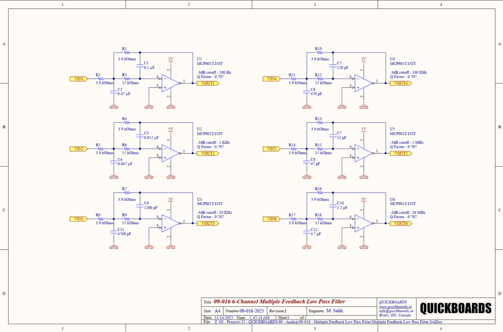
The core of this schematic consists of six independent 2nd-order active low pass filters utilizing the Multiple Feedback (MFB) topology. The MFB configuration was selected over Sallen-Key for its superior out-of-band rejection and reduced sensitivity to component tolerances. Each channel is configured with a Q-factor of 0.707 to achieve a Butterworth response, which ensures a maximally flat passband—a critical requirement for maintaining amplitude accuracy in data acquisition systems.
Signal Conditioning and Frequency Scaling
To simplify the bill of materials (BOM), the design standardizes resistor values across all six channels. The input and feedback resistors are set to 3.9 kOhms (R2, R1, etc.), while the intermediate stage resistors are set to 15 kOhms (R3, R6, etc.). This 3.9k/15k ratio is mathematically optimized to yield the desired Butterworth damping. Frequency tuning is performed solely by scaling the capacitor values (C1, C2, etc.) in decade steps. This approach allows for consistent phase response and noise characteristics across the 100 Hz to 10 MHz range while reducing assembly complexity.
Component Selection and Tolerances
For the resistive elements, 1% tolerance thick-film resistors are specified to minimize gain error and frequency shift. Capacitor selection is more specialized: for lower frequency channels (100 Hz to 10 kHz), X7R ceramic capacitors are used for their high volumetric efficiency. However, for the high-frequency channels (100 kHz, 1 MHz, and 10 MHz), C0G (NP0) dielectrics are mandatory. C0G capacitors provide near-zero temperature coefficients and negligible voltage coefficients, which are essential for maintaining the filter’s pole positions in precision analog signal chains.
Placement and Trace Logic
The physical layout requires the op-amp to be placed in close proximity to the MFB passive components. Specifically, the feedback capacitors (C1, C3, etc.) must have short, direct traces to the VOUT and VIN- pins to minimize parasitic inductance and capacitance. For the high-frequency channels, a solid ground plane should be maintained under the filter components to provide a low-impedance return path, but copper should be cleared away from the VIN- summing node to prevent stray capacitance from causing instability or peaking.
Design Rationale
Resistors R2 and R5 (3.9 kOhms) define the input impedance of each filter channel. This value provides a balance between minimizing thermal noise and ensuring that the signal source is not excessively loaded. The VIN+ pin (Pin 3) is tied directly to ground, defining the filter as an inverting stage. This configuration allows the op-amp to operate within its most linear region, providing predictable rail-to-rail performance.
Implementation Insights
A primary engineering consideration is the Gain Bandwidth Product (GBWP) limitation of the MCP601. While the schematic provides a 10 MHz channel (U6), the MCP601’s 2.8 MHz GBWP means the active filtering performance will degrade significantly as the signal approaches the cutoff. In practice, the 1 MHz and 10 MHz channels serve more as high-frequency suppressors than precise 2nd-order filters. For applications requiring an accurate Butterworth roll-off at 1 MHz and above, a high-speed op-amp with at least 50 MHz GBWP would be necessary.
Since the MFB topology is inverting, the output signal is 180 degrees out of phase with the input. This must be accounted for in the system software or subsequent analog stages. Additionally, while the MCP601 is rail-to-rail, designers should allow for approximately 20-50 mV of headroom from the rails to avoid clipping under maximum load conditions.
To ensure stability and low noise, a 0.1uF ceramic decoupling capacitor must be placed as close as possible to the VDD pin (Pin 5) of each op-amp. In multi-channel environments, a shared 10uF tantalum or electrolytic capacitor should also be present on the main supply rail to handle low-frequency transients.
Applications
- Automotive Sensor Conditioning: Filtering high-frequency switching noise from pressure and temperature sensors in engine control units.
- Portable Medical Devices: Providing anti-aliasing for heart rate monitors and battery-powered diagnostic tools.
- Industrial Process Control: Smoothing 4-20mA loop signals and removing electromagnetic interference (EMI) from factory floor sensors.
- Data Acquisition Systems: Functioning as a modular anti-aliasing front-end for microcontrollers and high-speed ADCs.
Integrating the MCP601T-I/OT into your design
This modular 6-channel MFB filter block simplifies the analog front-end by providing pre-calculated frequency windows that are production-ready. By standardizing the resistor networks and utilizing the low-power MCP601, this design eliminates the need for complex filter simulations and iterative component selection. This block ensures a flat passband and reliable roll-off across multiple decades of frequency, reducing first-spin risk in sensitive signal conditioning projects.
Skip the tedious research and manual entry. Download the production-ready schematic block for the MCP601T-I/OT directly from the Quickboards Library.