MCP601T-I/OT 8 Channel Active Low Pass Filter Reference Schematic Design
The MCP601T-I/OT is a single, rail-to-rail output operational amplifier designed by Microchip Technology. It is engineered for low-power, high-performance signal conditioning applications, operating with a single supply voltage as low as 2.7V. Its primary function in this modular block is to serve as an active buffer for a first-order low-pass filter array. This IC is frequently utilized in battery-powered instrumentation, sensor signal conditioning, and as an input buffer for Analog-to-Digital Converters (ADCs) where maintaining signal integrity with low output impedance is critical.
Overview of the Active Low Pass Filter
The MCP601 is part of a family of op-amps that offers a Gain Bandwidth Product (GBWP) of 2.8 MHz and a low typical operating current of only 230uA. By providing rail-to-rail output swing, it allows for maximum dynamic range even at low supply voltages. In this 8-channel active filter design, the MCP601 transforms passive RC networks into robust active stages, ensuring that the filter’s performance is not degraded by the input impedance of downstream components.
| Feature | Specification |
| Core Architecture | CMOS Operational Amplifier |
| Operating Voltage | 2.7V to 6.0V |
| Gain Bandwidth Product | 2.8 MHz |
| Slew Rate | 2.3 V/us |
| Input Offset Voltage | 2 mV (Maximum) |
| Output Type | Rail-to-Rail |
| Typical Quiescent Current | 230 uA |
| Package | 5-lead SOT-23 |
Pin Configuration and Function Mapping
The MCP601T-I/OT utilizes a standard 5-lead SOT-23 package, which is ideal for high-density modular breakout boards.
| Pin Number | Primary Function | Secondary / Peripheral Functions |
| 1 | VOUT | Output of the Operational Amplifier |
| 2 | VSS | Negative Power Supply / Ground |
| 3 | VIN+ | Non-inverting Input |
| 4 | VIN- | Inverting Input |
| 5 | VDD | Positive Power Supply |
Functional Block Analysis & Design Decisions
Signal Conditioning: Active First-Order Low Pass Filter
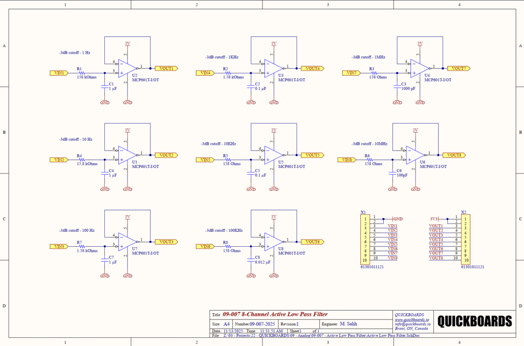
The primary functional block of this design is an 8-channel active filter array. Each channel consists of a passive RC network (Resistor and Capacitor) followed by an MCP601 configured as a unity-gain buffer (voltage follower). The RC network defines the -3dB cutoff frequency, while the op-amp provides the high input impedance required to prevent loading of the signal source and the low output impedance required to drive downstream loads without signal attenuation. This topology is chosen for its inherent stability and simplicity in multi-channel systems.
Component Selection: Precision and Frequency Scaling
Resistors R1 through R8 are selected from the E96 1% series (e.g., 158 Ohms, 1.58 kOhms, 15.8 kOhms, 158 kOhms). These values are calculated using the formula f = 1 / (2 * pi * R * C) to provide a wide spectrum of cutoff frequencies spanning from 1 Hz to 10 MHz. For low-frequency channels (1 Hz to 100 Hz), 1uF capacitors (C1, C4, C7) are used. As the cutoff frequency increases, the capacitance values scale down to 100pF for the 10 MHz channel (C6). For high-frequency stages (1 MHz and above), Ceramic C0G/NP0 capacitors are used instead of X7R types because of their superior temperature stability and lower voltage coefficient, ensuring the filter pole does not drift.
Placement & Trace Logic
The physical layout requires the RC components to be placed as close as possible to the non-inverting input (Pin 3) of the MCP601. This minimizes the length of the high-impedance trace, reducing its susceptibility to electromagnetic interference (EMI) and parasitic capacitance pickup. The output traces (VOUT1-VOUT8) are routed to the X2 header. Because the MCP601 has low output impedance, these traces can be longer than the input traces without significant signal loss, though they should still be kept away from high-frequency digital lines to prevent crosstalk.
Design Rationale: Unity-Gain Buffering
In each sub-circuit, the inverting input (Pin 4) is tied directly to the output (Pin 1). This creates a voltage follower configuration. The rationale behind this is to provide a power-efficient method of isolating sensitive sensor signals. By using an active buffer, the cutoff frequency defined by the RC network remains constant regardless of whether the output is connected to a 10k Ohm or a 1M Ohm load. This “plug-and-play” capability is essential for modular systems where the load characteristics may change.
Implementation Insights
When integrating the MCP601T-I/OT active filter block, ensure the 5V power rail is clean. Although not shown in individual channel views, a 0.1uF ceramic decoupling capacitor must be placed within 2mm of the VDD pin (Pin 5) of every op-amp to provide high-frequency current during signal transitions and maintain the 2.8 MHz bandwidth.
For the higher frequency channels (Channel 7 and 8), engineers must account for the Gain Bandwidth Product of the op-amp. Since the MCP601 has a GBWP of 2.8 MHz, it is perfectly suited for filtering signals up to the 1 MHz range (Channel 7). However, for the 10 MHz channel (Channel 8), the op-amp will act more as a limiter than a transparent buffer; this channel is primarily intended for applications where the passive RC roll-off is the primary concern and the op-amp is used to drive a high-impedance, low-capacitance load.
Applications
- Portable Instrumentation: Providing signal smoothing for handheld diagnostic tools where low power draw is mandatory.
- Battery-Powered Systems: Ideal for sensor interfaces in remote IoT nodes due to the low 230uA quiescent current.
- Sensor Signal Conditioning: Buffering high-impedance sensors like piezo-elements or photodiode transimpedance stages.
- Low-End Audio: Managing frequency limits in voice-band communication devices or basic audio playback systems.
Integrating the MCP601T-I/OT into your design
This modular active filter block simplifies the signal conditioning process by providing eight pre-validated frequency windows. By utilizing the MCP601 as a buffer, engineers eliminate the complex calculations associated with load-induced frequency shifts and gain errors. This design allows you to drop high-impedance filtering stages directly into your signal chain, ensuring that your ADC receives a clean, low-impedance signal ready for precision conversion.
Skip the tedious research and manual entry. Download the production-ready schematic block for the MCP601T-I/OT directly from the Quickboards Library.