MCP601T-I/OT 6 Channel Active Band Pass Filter Reference Schematic Design
The MCP601T-I/OT is a single, rail-to-rail output operational amplifier characterized by its low power consumption and wide operating voltage range. In the 09-009 modular block, this IC serves as the central isolation and buffering element in a multi-channel active wide band pass filter array. By cascading passive high-pass and low-pass stages with an active buffer, this design provides precise frequency windows while eliminating the loading effects that typically degrade passive-only filter networks. It is a fundamental building block for systems requiring signal cleanup, anti-aliasing, or specific frequency band isolation.
Overview of the Active Band Pass Filter
The MCP601 is designed for low-power applications, operating with a typical quiescent current of only 230uA. It features a Gain Bandwidth Product (GBWP) of 2.8 MHz, making it suitable for a variety of analog signal conditioning tasks. In the 09-009 reference design, the IC is utilized in a unity-gain configuration to provide high input impedance to a high-pass stage and low output impedance to a subsequent low-pass stage. This ensures that the two filter poles remain independent and deterministic across six decades of frequency.
| Feature | Specification |
| Operating Voltage | 2.7V to 6.0V |
| Gain Bandwidth Product | 2.8 MHz |
| Slew Rate | 2.3 V/us |
| Typical Quiescent Current | 230 uA |
| Input Offset Voltage | 2 mV (Maximum) |
| Output Type | Rail-to-Rail |
| Package Type | 5-Lead SOT-23 |
Pin Configuration and Function Mapping
The MCP601T-I/OT is housed in a compact 5-pin SOT-23 package, facilitating high-density layouts in modular sub-circuits.
| Pin Number | Primary Function | Secondary / Peripheral Functions |
| 1 | VOUT | Amplifier Output |
| 2 | VSS | Negative Power Supply / Ground |
| 3 | VIN+ | Non-inverting Input |
| 4 | VIN- | Inverting Input (Feedback) |
| 5 | VDD | Positive Power Supply (5V) |
Functional Block Analysis & Design Decisions
Active Wide Band Pass Topology
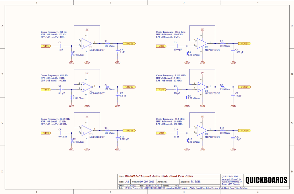
The 09-009 implements a cascaded architecture consisting of a first-order passive High-Pass Filter (HPF), an active unity-gain buffer, and a first-order passive Low-Pass Filter (LPF). This specific topology is chosen for its inherent stability and the ability to define wide passbands (10:1 frequency ratio) with minimal phase distortion. The active buffer is the critical link that prevents the second-stage LPF from loading the first-stage HPF, a common design requirement for maintaining accurate -3dB cutoff points in multi-stage analog filters.
High-Pass Stage and DC Blocking
The signal enters through a series capacitor (C1, C5, C9, etc.) and a shunt resistor to ground (R3, R7, R11, etc.). This stage performs the dual function of removing low-frequency noise (such as 50/60 Hz hum) and blocking DC offsets from the input source. In Channel 1, a 1uF capacitor and 1.58k resistor set the HPF cutoff at 100 Hz. For higher frequency channels, the values scale down to 10pF to achieve a 10 MHz HPF cutoff. The series capacitors are selected for their voltage ratings to ensure they can handle full-rail DC offsets.
Buffer and Isolation Stage
The MCP601 is configured as a voltage follower, with the inverting input tied directly to the output. This functional block provides near-infinite input impedance to the high-pass network. Senior engineers will recognize the importance of using a CMOS-input op-amp like the MCP601 here; its extremely low input bias current ensures that the high-value resistors in the low-frequency channels (e.g., 1.58k) do not create significant offset errors at the non-inverting input.
Low-Pass Stage and Signal Smoothing
The output of the buffer drives a series resistor (R1, R5, R9, etc.) and a shunt capacitor (C3, C7, C11, etc.). This stage removes high-frequency interference and serves as an anti-aliasing filter for downstream digitization. In Channel 1, the 158 ohm resistor and 1uF capacitor set the LPF cutoff at 1 kHz. The 10:1 ratio between the HPF and LPF cutoff frequencies creates a geometric center frequency (e.g., 316 Hz for Channel 1) that remains stable across temperature and component aging.
Component Selection
Resistor values are selected from the E96 1% series (158 ohm and 1.58k) to maintain high precision in the passband. For the low-frequency channels (100 Hz to 100 kHz), X7R ceramic capacitors are used for their balance of volumetric efficiency and stability. For the MHz-range channels (Channels 4, 5, and 6), C0G/NP0 dielectrics are utilized. These capacitors provide near-zero temperature coefficients and negligible voltage coefficients, which is vital for maintaining high-frequency pole accuracy in precision instrumentation.
Implementation Insights
A critical senior-level consideration for this block is the Gain Bandwidth Product (GBWP) of the MCP601. While the passive filter components in Channel 6 are calculated for a 10 MHz to 100 MHz passband, the 2.8 MHz GBWP of the MCP601 limits the active buffering capability to the low MHz range. In these high-frequency channels, the op-amp acts as a low-impedance node for the filter network, but the overall system bandwidth will be dominated by the IC’s internal poles. For applications requiring full transparency at 100 MHz, the buffer would require a high-speed alternative.
Grounding for the shunt capacitors (C3, C7, C11, etc.) must be exceptionally robust. These capacitors are the final path for high-frequency noise rejection. A solid, low-impedance ground plane is required to prevent ground-loop noise from being injected into the VOUT nodes. For the higher frequency channels, the shunt capacitors should be placed as close to the VOUT net as possible to minimize parasitic inductance.
Trace routing between the HPF stage and the VIN+ pin (Pin 3) should be kept short and isolated from digital clock lines. High-impedance analog nodes are highly susceptible to capacitive coupling, which can manifest as digital crosstalk in the filtered output signal.
Applications
- Sensor Signal Conditioning: Isolating specific frequency bands from industrial sensors while removing DC drift and high-frequency EMI.
- Audio Processing: Creating defined spectral windows for voice or instrument signals, removing sub-sonic rumble and ultrasonic artifacts.
- Communication IF Filtering: Providing wide-band signal isolation in intermediate frequency stages of radio and telecommunication systems.
- Instrumentation Front-Ends: Preparing low-level analog signals for ADC sampling by providing anti-aliasing and baseline stabilization.
Integrating the MCP601T-I/OT into your design
The 09-009 Active Wide Band Pass Filter block provides a production-ready, modular solution for complex frequency discrimination. By integrating the MCP601 as an isolation buffer, this design eliminates the iterative tuning and loading issues associated with passive cascaded filters. The standardized 10:1 bandwidth ratio and precision component selection ensure that this block can be dropped into any signal chain, providing predictable, high-fidelity results from DC to the MHz range.
Skip the tedious research and manual entry. Download the production-ready schematic block for the MCP601T-I/OT directly from the Quickboards Library.