LSM6DSOTR reference schematic design
The LSM6DSOTR is a high-performance, low-power 6-axis inertial measurement unit (IMU) featuring a 3D digital accelerometer and a 3D digital gyroscope. This iNEMO system-in-package is engineered for high-accuracy motion sensing in demanding applications. Its primary function is to provide precise motion and orientation data, which is essential for navigation, gesture recognition, and stabilization. It is widely utilized in handheld devices, wearables, and industrial automation where power efficiency and compact form factor are critical.
Overview of the LSM6DSOTR
The LSM6DSOTR offers an advanced feature set including an embedded pedometer, step detector, and tilt detection. It supports multiple communication interfaces, allowing for seamless integration with a variety of host processors. The internal signal processing provides filtered data at various rates, reducing the computational load on the external microcontroller.
| Technical Specification | Value |
| Supply Voltage (VDD) | 1.71V to 3.6V |
| I/O Voltage (VDDIO) | 1.62V to 3.6V |
| Accelerometer Full-Scale | +/- 2, 4, 8, 16 g |
| Gyroscope Full-Scale | +/- 125, 250, 500, 1000, 2000 dps |
| Communication Interfaces | I2C, SPI, MIPI I3C |
| Operating Temperature | -40 to +85 Celsius |
| Package Type | LGA-14 |
| Current Consumption | 0.55 mA in high-performance mode |
Pin Configuration and Function Mapping
The LSM6DSOTR is housed in a compact 14-pin land grid array (LGA) package. The pin mapping provided in this reference block ensures access to both the primary communication interface and auxiliary features for advanced sensor fusion.
| Pin Number | Primary Function | Secondary / Peripheral Functions |
| 1 | SDO/SA0 | SPI Serial Data Out / I2C Address LSB |
| 2 | SDx | Auxiliary Serial Data |
| 3 | SCx | Auxiliary Serial Clock |
| 4 | INT1 | Programmable Interrupt 1 |
| 5 | VDDIO | Supply Voltage for I/O Pins |
| 6 | GND | Ground Reference |
| 7 | GND | Ground Reference |
| 8 | VDD | Main Supply Voltage |
| 9 | INT2 | Programmable Interrupt 2 |
| 10 | OCS_Aux | Auxiliary OIS Serial Clock |
| 11 | SDO_Aux | Auxiliary OIS Serial Data Out |
| 12 | CS | SPI Chip Select / I2C Mode Selection |
| 13 | SCL | Serial Clock for I2C and SPI |
| 14 | SDA | Serial Data for I2C and SPI |
Functional Block Analysis & Design Decisions
Power and Decoupling Block
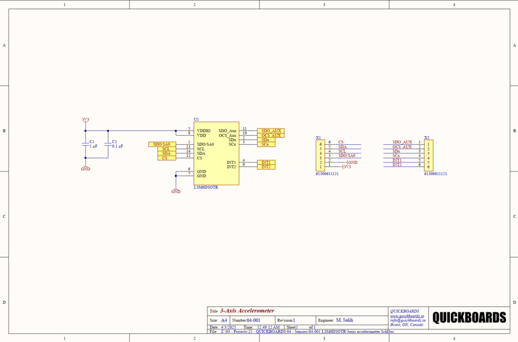
The power sub-circuit for the LSM6DSOTR involves the VDD and VDDIO rails. In this specific design, both pins 5 and 8 are tied to a common 3.3V supply (3V3). This simplifies the power tree for systems where logic levels match the main sensor supply. Decoupling is achieved through a tiered capacitor approach: C1 is a 1 microfarad bulk capacitor, and C2 is a 0.1 microfarad high-frequency bypass capacitor.
Component selection is critical here. Ceramic capacitors with X7R dielectrics are chosen for their excellent stability over temperature and voltage. The 0.1 microfarad capacitor (C2) is specifically sized to suppress high-frequency switching noise from the digital core, while the 1 microfarad capacitor (C1) handles lower-frequency load transients. These must be placed as close as possible to the IC supply pins to minimize parasitic inductance in the power path, which is vital for preventing erratic sensor readings or resets during high-performance operation.
Communication and Programming Interface
The digital interface block supports both I2C and SPI protocols through pins 1, 12, 13, and 14. By grounding or pulling up the CS pin, the user can define the default communication protocol. In this design, these signals are routed to a breakout connector (X1). The SDO/SA0 pin (Pin 1) provides flexibility in I2C mode, allowing the designer to change the least significant bit of the device address, effectively permitting two LSM6DSOTR sensors to reside on the same bus without conflict.
Signal Conditioning and Auxiliary IO
The schematic utilizes pins 2, 3, 10, and 11 for auxiliary data paths, broken out to header X2. These pins are intended for advanced use cases such as Optical Image Stabilization (OIS) or connecting a second auxiliary sensor (like a magnetometer) to the LSM6DSOTR internal hub. The programmable interrupts (INT1 and INT2) on pins 4 and 9 are designed to trigger the host processor only when specific motion events occur—such as free-fall, wake-up, or 6D orientation changes—thereby reducing total system power consumption.
Implementation Insights
When integrating this block, senior engineers must consider the mechanical orientation of the LGA package. Since the IC measures acceleration and angular rate along three axes, the physical placement on the PCB must be precisely aligned with the device’s chassis to avoid complex software-based rotation matrices.
A critical consideration is the handling of the SDO/SA0 pin. If this pin is left floating in I2C mode, the device address will be undefined, leading to communication failures. Ensure that Pin 1 is tied either to VDDIO or GND through a 0 Ohm resistor or a direct trace to define the bus address.
Mechanical stress on the LGA-14 package is another major design factor. Placing the sensor near PCB mounting holes or large heat-generating components can induce strain or thermal gradients that cause zero-g offset drift. Centering the sensor on the PCB and using symmetrical ground pours helps maintain the integrity of the inertial data over the product’s lifespan.
Applications
- Smartphones and Handhelds: Providing motion-based UI, portrait/landscape orientation, and gaming control.
- Wearable Devices: High-accuracy step counting, activity monitoring, and sleep analysis.
- Industrial Automation: Vibration monitoring in machinery and tilt sensing for heavy equipment.
- Optical Image Stabilization (OIS): Providing real-time angular rate data to camera modules for jitter reduction.
- Augmented and Virtual Reality: Low-latency head tracking and movement detection for immersive environments.
Integrating the LSM6DSOTR into your design
This modular block provides a validated hardware foundation for high-precision inertial sensing, significantly reducing the time required to calculate decoupling requirements and pin assignments. By utilizing a proven component set and standardized breakout headers, the design minimizes the risk of signal noise and communication errors often associated with first-spin sensor integration.
Skip the tedious research and manual entry. Download the production-ready schematic block for the LSM6DSOTR directly from the Quickboards Library.