CS43131 32bit Digital to Analog Reference Schematic Design
The CS43131-CNZR is a high-performance, 32-bit resolution stereo audio DAC featuring an integrated impedance-sensing headphone amplifier. This integrated circuit is designed to provide professional-grade audio fidelity in space-constrained applications such as smartphones, tablets, and portable DAC dongles. By combining a high-fidelity DAC with a ground-centered headphone driver, it eliminates the need for bulky DC-blocking capacitors, significantly reducing the total solution footprint while maintaining an ultra-low noise floor.
Overview of the CS43131-CNZR
The CS43131 acts as the primary signal conversion and amplification stage in high-end portable audio chains. It is favored for its class-leading 130 dBA dynamic range and -115 dB THD+N performance. Typical applications include high-fidelity mobile devices, battery-powered headphone amplifiers, and premium portable media players.
| Feature | Specification |
| Core Architecture | 32-bit Delta-Sigma DAC |
| Max Sample Rate | 384 kHz (PCM) / DSD256 |
| Dynamic Range | 130 dBA |
| THD + N | -115 dB |
| Operating Voltage (VL) | 1.8V |
| Digital Interface | I2C (Control), I2S/TDM/DSD (Data) |
| Output Type | Ground-Centered Stereo Headphone |
| Package | 40-pin WLCSP / QFN |
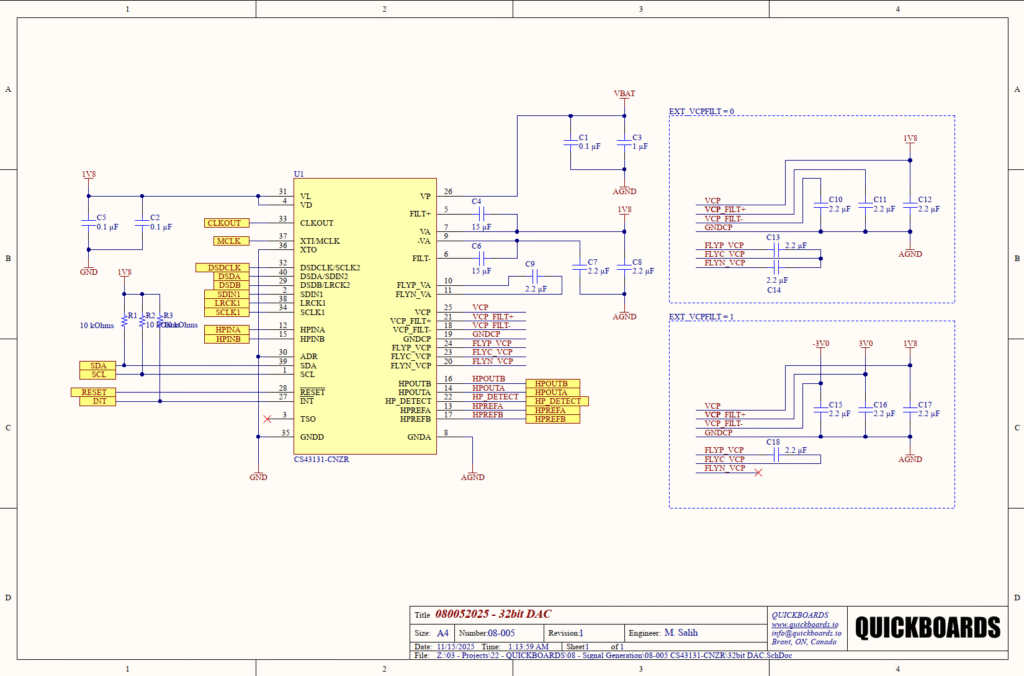
Pin Configuration and Function Mapping
The CS43131-CNZR provides a dense mapping of digital control, high-speed data, and sensitive analog power nodes required for low-noise audio conversion.
| Pin Number | Primary Function | Secondary / Peripheral Functions |
| 31, 4 | VL / VD | Digital Core and I/O Power Supply (1.8V) |
| 26 | VP | Battery/Power Input (VBAT) |
| 7, 9 | VA / -VA | Positive/Negative Analog Supply (Charge Pump Output) |
| 5, 6 | FILT+ / FILT- | Analog Filter Reference Nodes |
| 37, 36 | XTI/MCLK / XTO | External Master Clock / Crystal Input |
| 1, 39 | SCL / SDA | I2C Control Interface |
| 38, 34 | LRCK1 / SCLK1 | Digital Audio Interface (WS and BCLK) |
| 2, 29 | SDIN1 / SDIN2 | Digital Audio Data Input (Stereo Channels) |
| 14, 16 | HPOUTA / HPOUTB | Left/Right Headphone Output |
| 22 | HP_DETECT | Headphone Jack Insertion Detection |
Functional Block Analysis & Design Decisions
Power Management & Decoupling Block
The schematic implements a multi-rail power strategy to isolate digital switching noise from the sensitive analog DAC core. The digital supply (VL/VD) is decoupled using 0.1uF ceramic capacitors (C5, C2), while the battery input (VBAT/VP) uses a dual-capacitor approach with 0.1uF (C1) and 1uF (C3) ceramic capacitors. The 0.1uF capacitors are selected for their low Equivalent Series Inductance (ESL) to filter high-frequency transients, while the 1uF bulk capacitor handles lower-frequency load steps. These must be placed as physically close to the VP and VL pins as possible to minimize parasitic trace inductance.
Analog Filtering & Reference Block
The FILT+ (Pin 5) and FILT- (Pin 6) pins are the primary reference nodes for the DAC’s internal analog circuitry. The design utilizes 15uF ceramic capacitors (C4, C6) for these nodes. The unusually high value of 15uF is a technical requirement for achieving the 130 dBA dynamic range, as these capacitors act as the final stage of noise rejection for the internal analog reference voltage. To maintain performance, these should be high-quality X7R or X5R dielectrics with low leakage current.
Headphone Charge Pump & VCP Block
The CS43131 features an integrated Class H charge pump to generate the bipolar (VA and -VA) rails for the headphone amplifier. This allows for a ground-centered output. The schematic shows two possible configurations for the VCP filter network (EXT_VCPFILT = 0 or 1). The design utilizes 2.2uF capacitors (C7-C18) for the flying capacitor (FLYP/FLYN) and reservoir nodes (VCP).
The choice of 2.2uF ensures a balance between low output impedance for the power rails and fast startup time. These capacitors must be placed with high-priority routing; the FLYP/FLYN loops carry high di/dt currents and should be kept as compact as possible to prevent Electromagnetic Interference (EMI) from coupling into the audio output.
Digital Audio & Control Interface
The digital section manages I2C control and high-speed I2S data. R1, R2, and R3 (10 kOhms) serve as pull-up resistors for the SDA, SCL, and RESET lines. This value ensures that the bus rise times comply with the 400 kHz I2C Fast-mode specification while minimizing static power consumption. The digital data lines (SDIN, SCLK, LRCK) are routed directly to the system processor.
Implementation Insights
A primary engineering consideration for the CS43131 is the grounding strategy. This is a mixed-signal IC that requires a star-grounding technique where the analog ground (AGND) and digital ground (GND) planes meet at a single point, typically the exposed pad of the IC or a dedicated ground bridge.
Failing to isolate the digital return currents from the analog reference capacitors (C4, C6) will result in audible “hum” or “buzz” as digital switching noise modulates the analog reference.
Another significant consideration is the headphone detection logic. Pin 22 (HP_DETECT) should be connected to a normally-closed or normally-open switch on the headphone jack. Proper debounce logic should be implemented in the host firmware to prevent false trigger events during jack insertion, which could lead to loud audible pops if the amplifier is enabled prematurely.
Designers must be cautious with the routing of the 1.8V VL rail. Since this rail powers the digital I/O and parts of the analog core, noise on this rail can directly affect the jitter performance of the internal clock. It is advisable to use a dedicated low-noise LDO for the VL rail rather than a shared switching regulator output.
Applications
- Smartphones: Provides high-resolution audio output through the USB-C port or integrated jack while minimizing battery drain.
- Portable Headphone Amplifiers: Serves as the core DAC and driver for high-impedance audiophile headphones in a compact form factor.
- Tablets and Laptops: Upgrades the standard integrated audio path to professional-grade high-fidelity specifications.
- DAC Dongles: The high level of integration makes it the ideal solution for ultra-portable USB-C to 3.5mm adapters.
Integrating the CS43131-CNZR into your design
This modular block provides a pre-validated hardware environment for the CS43131-CNZR, managing the complexities of the ground-centered charge pump and the high-precision analog filtering requirements. By utilizing this sub-system, engineers eliminate the risk of noise-floor degradation and power-sequencing errors that often occur during the first spin of high-fidelity audio designs.
Skip the tedious research and manual entry. Download the production-ready schematic block for the CS43131-CNZR directly from the Quickboards Library.