AS72651, AS72652, and AS72653 multispectral color sensor reference schematic design
The AS7265x chipset is a revolutionary three-sensor multispectral solution consisting of the AS72651 (Master/NIR), AS72652 (Visible), and AS72653 (UV) integrated circuits. When combined, these sensors create an 18-channel spectrophotometer capable of sensing light from the ultraviolet (350 nm) through the visible spectrum into the near-infrared (940 nm). This modular chipset is designed for complex optical analysis tasks, such as material identification, agricultural monitoring, and product authentication. Each sensor in the triad features integrated independent LED drivers and factory-calibrated optical filters, providing a production-ready laboratory-on-a-chip environment for high-precision spectroscopic measurements.
Overview of the AS7265x Chipset
The architecture of this chipset relies on a Master-Slave configuration where the AS72651 (U1) acts as the primary interface hub for the host system, managing data acquisition from the AS72652 (U2) and AS72653 (U3) via a private internal bus. This design allows the host to interact with a single logical device while accessing 18 discrete spectral channels. Possible applications range from handheld food freshness analyzers to industrial fluid contamination sensors and advanced color matching systems.
| Technical Specification | Details |
| Spectral Range | 350 nm to 940 nm (18 Channels) |
| Channel Bandwidth | 20 nm (Full Width at Half Maximum) |
| Supply Voltage | 2.7V to 3.6V |
| Host Communication | I2C, UART, or SPI |
| Integrated LED Drivers | 3 Independent Channels (Up to 100 mA each) |
| ADC Resolution | 16-bit per channel |
| Calibration | Factory-normalized spectral response |
| Package Type | 20-pin LGA |
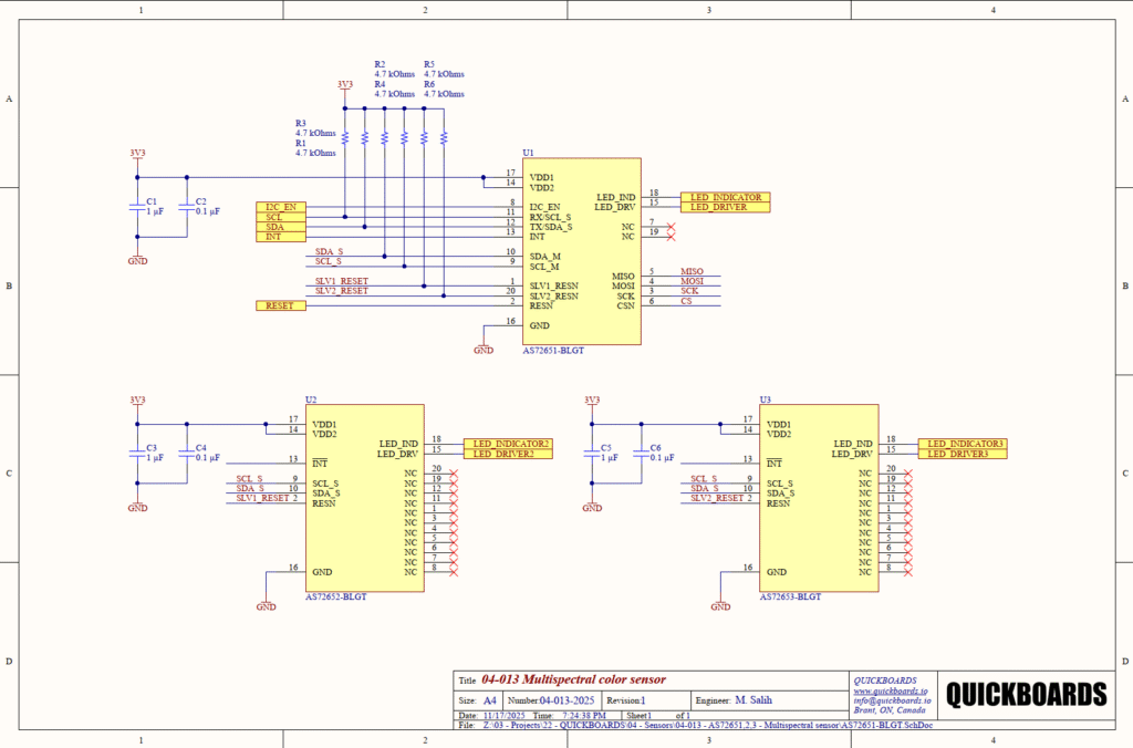
Pin Configuration and Function Mapping
The following mapping describes the primary functions of the AS72651 Master IC and the interconnected slave sensors.
| Pin Number | Primary Function | Secondary / Peripheral Functions |
| 17, 14 | VDD1 / VDD2 | Main Power Supply Pins (3.3V) |
| 16 | GND | Common Ground Reference |
| 11 | I2C_EN | I2C / UART Selection (High = I2C) |
| 12, 13 | RX/SCL_S, TX/SDA_S | Host Interface (I2C/UART) |
| 9, 10 | SCL_M, SDA_M | Internal Master-Slave I2C Bus |
| 1, 20 | SLV1_RESN, SLV2_RESN | Slave Sensor Reset Control |
| 2 | RESN | Main Hardware Reset (Active Low) |
| 15 | LED_DRV | Programmable Spectral Illumination Driver |
| 18 | LED_IND | System Status / Flash Indicator Driver |
| 3, 4, 5, 6 | SCK, MOSI, MISO, CSN | SPI Digital Interface |
Functional Block Analysis & Design Decisions
Power and Decoupling Block
In this multispectral array, each sensor (U1, U2, U3) is provided with its own dedicated decoupling network. The VDD1 and VDD2 rails are supported by a parallel combination of a 1 uF capacitor (C1, C3, C5) and a 0.1 uF capacitor (C2, C4, C6). Multispectral sensors are highly sensitive to power supply noise, which can manifest as jitter or measurement offsets in the 16-bit ADC stages. The 0.1 uF ceramic capacitors provide a low-impedance path to ground for high-frequency digital switching noise, while the 1 uF capacitors act as localized bulk energy reservoirs. The use of X7R ceramic capacitors is specified for their excellent capacitance stability across the industrial temperature range compared to standard electrolytic types.
Chipset Interconnectivity (Master-Slave Bus)
The AS72651 manages the secondary sensors through a private internal I2C bus (SCL_M, SDA_M connected to SCL_S, SDA_S). To ensure robust signal timing and prevent data corruption during rapid spectral acquisitions, 4.7 kOhm pull-up resistors (R2, R4, R5, R6) are utilized on these lines. This value is chosen as a senior-level standard for 400 kHz I2C operation, providing a fast enough rise time to comply with bus timing while minimizing static current draw. By isolating this bus from the main host interface, the design prevents external bus traffic from interfering with the precise timing required for multi-chip sensor fusion.
Reset Management and Synchronization
To ensure a deterministic startup sequence, the AS72651 Master IC controls the hardware reset pins (RESN) of the visible and UV sensors via the SLV1_RESET and SLV2_RESET nets. This allows the master firmware to synchronize the initialization of all 18 channels. A 4.7 kOhm pull-up resistor (R1, R3) is provided on the reset lines to define a stable default operating state. This hardware-level control is essential for preventing “ghosting” or communication timeouts if one sensor in the triad undergoes a brown-out event or fails to initialize simultaneously with the master.
Integrated Illumination Control
The schematic utilizes the LED_DRV and LED_IND pins for each sensor. These pins are designed to sink current for spectral illumination LEDs. Because the optical filters on the chipset are passive, accurate spectroscopic measurements require controlled, repeatable light sources. The internal drivers are programmable constant-current sinks, which eliminate the need for external drive transistors and ensure that the LED output intensity remains consistent even if the battery voltage fluctuates, which is paramount for maintainable factory calibration.
Implementation Insights
A primary engineering consideration for the AS7265x chipset is optical path mechanical alignment. Because the UV, Visible, and NIR sensors are discrete components, the PCB layout must place them as closely together as possible to minimize parallax errors. If the sensors are widely separated, the field of view for each channel will overlap differently on the target material, potentially leading to inaccurate spectral reconstruction for non-uniform samples.
Another consideration involves the thermal management of the LED drivers. When all three sensors are active and driving spectral LEDs at high current (up to 100 mA each), significant localized heating can occur. Senior designers should utilize thermal vias to connect the GND pads (Pin 16) to a large internal ground plane to act as a heat sink. Excessive heat can induce thermal drift in the integrated optical filters, shifting the center wavelength of the 18 channels.
Finally, manage the I2C_EN pin logic carefully. In this reference block, the master is configured for I2C communication. If a UART interface is preferred for long-cable or remote sensing applications, the I2C_EN pin must be tied to GND during power-up. This selection is latched during initialization and cannot be changed dynamically, requiring a hardware-level strap or a GPIO-controlled line from the host MCU.
Applications
- Agricultural Spectroscopy: Non-destructive testing of plant health and chlorophyll content using UV and NIR spectral signatures.
- Product Authentication: Detecting anti-counterfeiting markers in luxury goods or pharmaceuticals through specific spectral absorption patterns.
- Environmental Analysis: Real-time monitoring of water quality, oil contamination, or air particulate composition in industrial environments.
- Medical Diagnostics: Portable analysis of skin health or biochemical indicators via non-invasive spectral reflection measurements.
- Food and Beverage Monitoring: Assessing the ripeness of fruit or the authenticity of high-value liquids like olive oil and honey.
integrating the AS7265x into your design
The AS72651, AS72652, and AS72653 multispectral modular block provides a validated, production-ready environment for complex optical analysis. By utilizing this pre-tested triad architecture, engineers eliminate the risks associated with multi-chip bus timing, synchronized reset management, and ratiometric supply decoupling. This building block enables teams to bypass the fundamental physics of spectrophotometer design and focus immediately on the spectral algorithms and material identification logic required for their specific application.
Skip the tedious research and manual entry. Download the production-ready schematic block for the AS72651, AS72652, and AS72653 directly from the Quickboards Library.