AP3012KTR-G1 12-24V Boost Converter Reference Schematic Design
The AP3012KTR-G1 is a high-frequency, constant-frequency step-up DC/DC converter designed for applications requiring a compact footprint and high efficiency. Operating at a fixed switching frequency of 1.5MHz, this IC allows for the use of small-sized external inductors and capacitors, making it ideal for space-constrained designs. It is typically employed in providing bias voltages for LCD panels, driving white LED backlights, or generating higher voltage rails from low-voltage battery sources in portable electronics.
Overview of the AP3012KTR-G1
The AP3012 utilizes a peak current mode control scheme to regulate the output voltage. With a built-in 500mA MOSFET and a wide input voltage range, it can generate output voltages up to 29V. Its high switching frequency is a strategic choice to push switching noise into a frequency band that is easier to filter, which is a significant advantage in sensitive analog or communication systems.
| Feature | Specification |
| Input Voltage Range | 2.6V to 16V |
| Maximum Output Voltage | 29V |
| Switching Frequency | 1.5 MHz |
| Feedback Voltage | 1.25V |
| Switch Current Limit | 500mA |
| Shutdown Current | < 1uA |
| Package | SOT-23-5 |
Pin Configuration and Function Mapping
The AP3012KTR-G1 is housed in a 5-pin SOT-23 package, which minimizes PCB real estate while providing all necessary control and power paths.
| Pin Number | Primary Function | Secondary / Peripheral Functions |
| 1 | SW | Switching Node (Internal MOSFET Drain) |
| 2 | GND | Ground Reference |
| 3 | FB | Feedback Input (1.25V Reference) |
| 4 | SHDN | Active High Shutdown Control |
| 5 | VIN | Input Supply Voltage |
Functional Block Analysis & Design Decisions
Power Conversion Stage (Boost Topology)
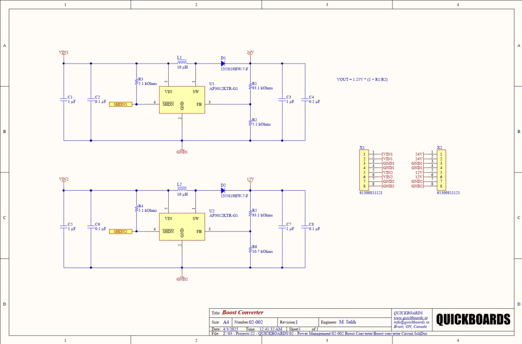
The core of this modular block is the asynchronous boost topology consisting of L1/L2, the internal switch at the SW pin, and the external Schottky diode D1/D2. We have selected a 10uH inductor for both the 12V and 24V rails. At a 1.5MHz switching frequency, 10uH provides an optimal balance between minimizing peak-to-peak ripple current and keeping the physical size of the component small. The 1N5819HW-7-F Schottky diode was chosen for its fast switching speed and low forward voltage drop (Vf), which is paramount for maximizing conversion efficiency in an asynchronous converter.
Input and Output Decoupling
The schematic employs a dual-capacitor strategy for both input (C1/C2, C5/C6) and output (C3/C4, C7/C8) stages. We use a 1uF ceramic capacitor in parallel with a 0.1uF capacitor. While the 1uF capacitor provides the bulk energy storage needed to handle switching transients, the 0.1uF capacitor is critical for high-frequency noise rejection. Ceramic capacitors with X7R or X5R dielectrics are specified here due to their low equivalent series resistance (ESR) and stability over temperature, which prevents voltage ringing at the SW node.
Voltage Regulation and Feedback
The output voltage is defined by the resistive divider network at the FB pin. The AP3012 maintains the FB pin at a constant 1.25V. By using the formula VOUT = 1.25V * (1 + R1/R2), we have configured two standard rails: 24V (using 93.1k and 5.1k) and 12V (using 93.1k and 10.7k). These resistor values are chosen from the E96 series to achieve high set-point accuracy. Senior engineers will note that the feedback resistors are kept in the kilo-ohm range to balance noise immunity with minimal quiescent current draw.
Shutdown and Logic Control
The SHDN pin is the interface for system-level power management. In this design, R3 and R4 (5.1k) act as pull-up resistors to VIN, ensuring that the converter is enabled by default. This “fail-safe” configuration allows the block to function immediately upon power-up unless an external microcontroller explicitly pulls the SHDN1/SHDN2 signals low to enters a low-power state.
Implementation Insights
Layout is the single most important factor in the success of a 1.5MHz boost converter. The “power loop”—defined by the path from the SW pin, through the Schottky diode, into the output capacitor, and back to the GND pin—must be kept as short and wide as possible. High-frequency current pulses in this loop can generate significant EMI and voltage spikes if trace inductance is not minimized.
The feedback trace (connected to pin 3) must be routed away from the SW node (pin 1). The SW node is a high-dv/dt point that can capacitively couple noise into the high-impedance feedback path, leading to output instability or jitter. For multi-layer boards, it is recommended to place a solid ground plane directly beneath the IC to act as a thermal sink and provide a low-impedance return path for the high-frequency switching currents.
Applications
- LCD Bias Power Supplies: Provides the positive high-voltage rails required for active-matrix liquid crystal displays.
- White LED Drivers: Ideal for driving strings of LEDs in series for backlighting applications where uniform current is necessary.
- Digital Cameras and Handheld GPS: Efficiently boosts single or dual-cell battery voltages to drive internal subsystems.
- Portable Media Players: Used for generating auxiliary rails from Li-Ion batteries in small-form-factor consumer devices.
Integrating the AP3012KTR-G1 into your design
This modular block simplifies the integration of boost power stages by providing pre-calculated component values for the two most common industrial voltage rails. By utilizing a fixed-frequency architecture and pre-selected Schottky and inductor components, this design eliminates the trial-and-error often associated with DC/DC stability and ripple management. The breakout headers X1 and X2 allow for immediate bench testing and seamless connection to a main system controller.
Skip the tedious research and manual entry. Download the production-ready schematic block for the AP3012KTR-G1 directly from the Quickboards Library.