ACS781KLRTR-150U-T 150A Current Sensor Reference Schematic Design
The ACS781KLRTR-150U-T is a high-precision, Hall-effect-based linear current sensor IC designed for high-current sensing in automotive and industrial applications. This device features a low-resistance integrated conductor that allows for the measurement of up to 150A. The primary function of the IC is to provide a ratiometric analog output voltage that is proportional to the current flowing through the primary conduction path. Typical applications include electric vehicle (EV) motor control, battery management systems (BMS), power distribution units, and solar inverters, where accurate high-current monitoring and galvanic isolation are essential.
The “U” suffix in the part number indicates a unipolar configuration, meaning the sensor is optimized for current flowing in a single direction, providing a wider dynamic range for applications such as battery charging or DC motor drives. By utilizing an internal differential sensing technique, the ACS781 provides excellent immunity to external stray magnetic fields, a critical requirement in dense power electronic environments.
| Technical Specification | Value |
| Supply Voltage (VCC) | 3.0V to 3.6V |
| Measurement Range | 150A (Unipolar) |
| Isolation Voltage | 2100 Vrms |
| Typical Sensitivity | 13.3 mV/A |
| Bandwidth | 120 kHz |
| Conductor Resistance | 200 micro-Ohms |
| Response Time | 3.6 microseconds |
| Operating Temperature | -40 to 125 degrees Celsius |
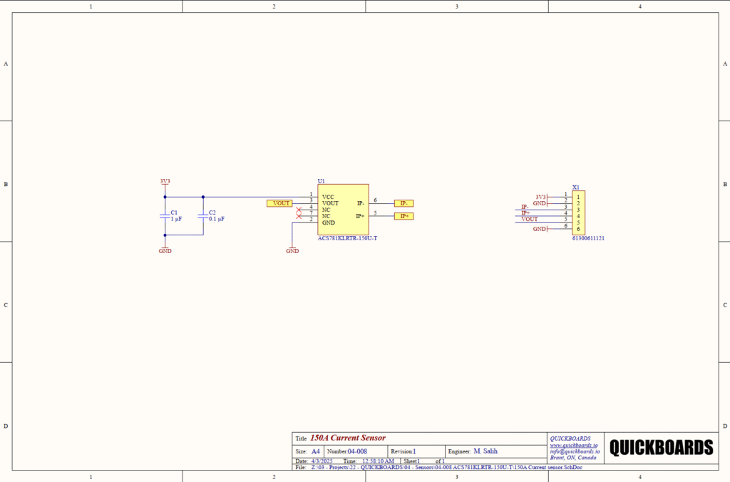
Pin Configuration and Function Mapping
The ACS781 is housed in a specialized 7-pin LR package designed to handle significant current loads while maintaining appropriate creepage and clearance distances for safety.
| Pin Number | Primary Function | Secondary / Peripheral Functions |
| 1 | VCC | Positive Power Supply Input |
| 2 | GND | Device Ground Reference |
| 3 | VOUT | Analog Output Voltage |
| 4, 7 | NC | No Internal Connection (Mechanical Support) |
| 5 | IP+ | Positive Current Input Terminal |
| 6 | IP- | Negative Current Input Terminal |
Functional Block Analysis & Design Decisions
Power and Decoupling Block
The power sub-circuit focuses on Pin 1 (VCC), which is tied to the 3.3V (3V3) rail. High-accuracy Hall-effect sensors are sensitive to power supply fluctuations as their output is ratiometric to the input voltage. This design employs a tiered decoupling strategy using C1 (1 micro-Farad) and C2 (0.1 micro-Farad). The 0.1 micro-Farad capacitor acts as a high-frequency bypass, selected for its low equivalent series inductance (ESL) to shunt fast switching noise generated by high-power semiconductors in the system. The 1 micro-Farad capacitor provides localized bulk storage to maintain voltage stability during load transients. Ceramic X7R capacitors are specified due to their superior thermal stability and aging characteristics compared to electrolytic alternatives.
High-Current Conduction Path (IP+ / IP-)
The primary current path is handled through Pins 5 and 6. The internal copper conductor has an extremely low resistance of approximately 200 micro-Ohms. This design choice is paramount for minimizing power dissipation ($P = I^2 \times R$) and self-heating when operating at the full 150A rating. In the schematic, these terminals are broken out to a high-current connector (X1). Senior engineers must ensure the physical PCB layout utilizes heavy copper weights (3 oz or higher) and wide, multi-layer pours to transition current into these pins to avoid localized heating that could exceed the package’s thermal limits.
Signal Conditioning and Output
The VOUT pin (Pin 3) delivers the analog representation of the current. Since this is a unipolar sensor, the zero-current output voltage is typically set at 0.33V (when $VCC = 3.3V$), allowing the full remaining voltage swing to represent the 0 to 150A range. The trace logic for VOUT should be kept away from high-speed digital lines to prevent capacitive coupling of switching noise into the analog signal. A solid ground reference at Pin 2 is essential for providing a stable return path for the output signal to the host ADC.
Placement & Trace Logic
The physical layout requirements for this block are stringent due to the 150A current requirement. The decoupling capacitors C1 and C2 must be placed within 2mm of Pin 1 to ensure effective noise filtering. Isolation is another key layout consideration; although the IC provides internal isolation, the PCB layout must maintain the clearance between the high-current side (Pins 5-6) and the low-voltage side (Pins 1-3) to comply with safety standards. Solid copper planes connected to the IP pins serve a dual purpose as both electrical conductors and primary heat sinks for the IC.
Implementation Insights
A primary engineering consideration for the ACS781 is the ratiometric nature of the output. Because VOUT scales with VCC, any noise or voltage drop on the 3.3V regulator will translate directly into a measurement error at the host ADC. For high-precision applications, it is advisable to share the same reference voltage between the sensor’s VCC and the ADC’s reference pin to nullify common-mode supply variations.
Thermal management is the second major consideration. Even with a 200 micro-Ohm internal resistance, a 150A continuous load will generate 4.5 Watts of heat within the IC package. Without adequate thermal relief and copper surface area on the PCB, the device will rapidly reach its thermal shutdown point. Utilizing large thermal vias to internal planes can help distribute this heat throughout the board.
Magnetic crosstalk is a persistent challenge in high-current designs. While the ACS781 uses differential sensing to reject common-mode fields, nearby busbars carrying hundreds of amps can still induce a differential field if they are placed asymmetrically relative to the sensor. The sensor should be placed such that external current-carrying traces are at a distance or oriented perpendicular to the sensor’s sensing axis.
Applications
- EV Traction Inverters: Real-time phase current monitoring for motor control loops to ensure efficient torque delivery.
- Battery Management Systems (BMS): Accurate tracking of battery discharge currents to calculate state-of-charge (SoC) and protect against over-current events.
- Photovoltaic (PV) Inverters: Monitoring the DC string current in solar arrays to optimize power point tracking (MPPT).
- Industrial Welding Equipment: Precise control of high-current output for welding arc stability.
- Power Distribution Units (PDU): Load monitoring in data center power rails to manage energy distribution and redundancy.
Integrating the ACS781KLRTR-150U-T into your design
This modular block provides a validated, production-ready solution for high-current monitoring up to 150A. By utilizing the specific decoupling values and standardized conduction path mapping provided here, engineers can eliminate the uncertainty associated with power integrity and thermal management in Hall-effect sensing. This reusable building block ensures that the sensitive analog output is protected from system noise while providing a robust mechanical and electrical interface for high-power buses.
Skip the tedious research and manual entry. Download the production-ready schematic block for the ACS781KLRTR-150U-T directly from the Quickboards Library.