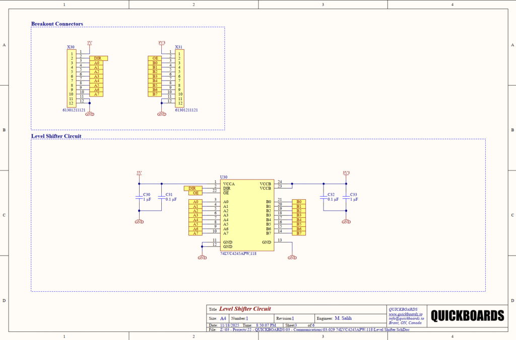
74LVC4245APW,118 Level Shifter Reference Schematic Design
The 74LVC4245APW,118 is an 8-bit, dual-supply translating transceiver designed to interface between systems operating at different logic levels. Its primary function is to provide asynchronous bidirectional data communication between a 5V bus and a 3.3V bus. In the modern landscape of embedded design, where low-power 3.3V microcontrollers frequently must interact with legacy 5V industrial sensors or displays, this IC serves as a critical bridge. Its high-drive capability and low propagation delay make it suitable for high-speed data buses and backplane interfaces.
Overview of the 74LVC4245APW,118
The device features two separate supply rails: VCCA, which is typically tied to the 5V system, and VCCB, which is tied to the 3.3V system. This dual-rail architecture ensures that the logic levels on each side of the transceiver are correctly matched to their respective environments. The direction of data flow is controlled by a single direction-control (DIR) input, while the output-enable (OE) input allows the designer to put the entire bus into a high-impedance state for system isolation or power saving.
| Feature | Specification |
| Core Architecture | Dual-Supply Translating Transceiver |
| VCCA Supply Range | 4.5V to 5.5V |
| VCCB Supply Range | 2.7V to 3.6V |
| Data Bus Width | 8-Bit |
| Output Drive | 24 mA |
| Propagation Delay | 6.7 ns (Typical at 5V/3.3V) |
| Operating Temperature | -40 to +125 degrees Celsius |
Pin Configuration and Function Mapping
The 74LVC4245APW utilizes a 24-pin TSSOP package. The mapping below reflects the standard configuration for a 5V to 3.3V translation block as seen in the provided reference schematic.
| Pin Number | Primary Function | Secondary / Peripheral Functions |
| 1 | VCCA | 5V Logic Side Power Supply |
| 2 | DIR | Direction Control Input |
| 3 – 10 | A0 – A7 | 5V Side Data Inputs / Outputs |
| 11, 12, 13 | GND | System Ground |
| 14 – 21 | B7 – B0 | 3.3V Side Data Inputs / Outputs |
| 22 | OE | Output Enable (Active Low) |
| 24 | VCCB | 3.3V Logic Side Power Supply |
Functional Block Analysis & Design Decisions
Dual-Supply Power and Decoupling
This block features two independent power domains. VCCA is supplied by the 5V rail, while VCCB is supplied by the 3.3V rail. To ensure signal integrity and suppress switching transients, each supply pin is equipped with a tiered decoupling strategy: a 0.1uF ceramic capacitor (C31, C32) and a 1uF bulk capacitor (C30, C33). The 0.1uF capacitors are selected for their low equivalent series resistance (ESR) and high-frequency response, filtering out the rapid noise generated by the high-speed switching of the 8-bit bus. The 1uF capacitors provide a local reservoir to handle lower-frequency load steps.
For optimal performance, these capacitors must be placed as physically close to the VCCA (Pin 1) and VCCB (Pin 24) pins as possible. Using Ceramic X7R dielectrics is mandatory for this application to maintain stable capacitance over the industrial temperature range and voltage fluctuations.
Direction and Enable Control Logic
The DIR and OE pins are high-impedance CMOS inputs that define the state of the transceiver. In this design, these pins are broken out to the system headers, allowing an external microcontroller to manage bus directionality and isolation. A low signal on OE enables the outputs, while a high signal places the A and B ports into a high-impedance state. This is particularly useful during system power-up to prevent bus contention or floating signals from reaching sensitive inputs. No pull-up resistors are included on these lines within the block to allow for maximum flexibility, though the driving host should ensure these lines are never left floating.
Bidirectional Data Bus Interface
The A-port (5V) and B-port (3.3V) interface pins are designed for high-speed operation. To minimize signal reflections and crosstalk, the traces for A0-A7 and B0-B7 should be routed with matched lengths and consistent impedance. The schematic shows these ports broken out through J1 and J2 (X30, X31) connectors. Because the 74LVC4245A has a high output drive (24 mA), it can drive relatively long traces or backplanes, but the designer must be mindful of the increased power consumption and EMI associated with high-drive switching.
Implementation Insights
When integrating this level shifter, the power-up sequence is an essential consideration. While the 74LVC4245A is designed to be robust, it is a standard practice to ensure that both VCCA and VCCB are stable before attempting to toggle the OE line to avoid transient logic states. Furthermore, because this is an asynchronous transceiver, the propagation delay is the only significant timing constraint; ensure that the system’s data-valid window accounts for the approximately 7 ns delay added by the translation stage.
One oversight often encountered is the handling of unused pins. While this block provides access to all 8 bits, if your design only requires 4 bits of translation, the unused input pins on the driving side must be tied to a valid logic level (GND or VCC) to prevent internal oscillation and excessive quiescent current consumption.
Applications
- Industrial Control Systems: Interfacing modern 3.3V controllers with legacy 5V PLCs and motor drivers.
- Workstations and Servers: Providing level translation for various communication buses on a motherboard.
- Telecommunications Equipment: Bridging different voltage domains in high-density network switches.
- Consumer Electronics: Connecting 3.3V application processors to 5V peripheral modules or displays.
Integrating the 74LVC4245APW,118 into your design
This modular block provides a pre-validated, layout-ready solution for bidirectional 8-bit level translation. By utilizing this sub-system, designers eliminate the complexities of dual-supply decoupling and ensure that the critical timing characteristics of the level translation stage are respected. The standardized breakout configuration allows for immediate integration into larger systems, providing a reliable path for high-speed data between mismatched voltage domains.
Skip the tedious research and manual entry. Download the production-ready schematic block for the 74LVC4245APW,118 directly from the Quickboards Library.