6-Channel Passive Wide Band Pass Filter Reference Schematic Design
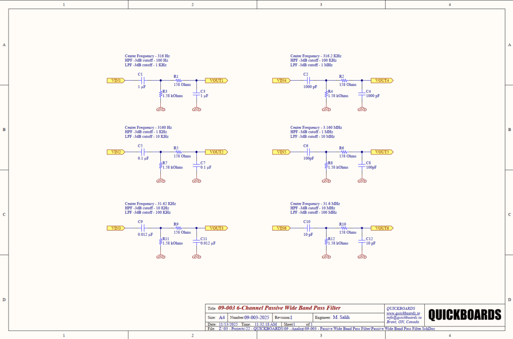
The 09-003 is a modular 6-channel passive signal conditioning block designed for precision wide-band filtering across a massive frequency spectrum. By utilizing a cascaded passive architecture, this block provides localized frequency discrimination from 100 Hz up to 100 MHz without the power requirements, DC offsets, or noise floors associated with active operational amplifier topologies. It is typically employed in multi-sensor data acquisition systems, high-speed communication front-ends, and industrial noise-rejection circuits where signal integrity and power efficiency are primary design constraints.
Overview of the Band Pass Filter
The filter functions as a frequency-selective window, allowing only a specific range of frequencies to pass while attenuating unwanted out-of-band signals. Each of the six channels is configured as a “wide” band pass filter, meaning the low-pass and high-pass cutoff frequencies are separated by exactly one decade (a 10:1 ratio). This results in a flat response across the intended signal bandwidth and a geometric mean center frequency that remains highly stable. Because the block is entirely passive, it is inherently bi-directional and linear, making it suitable for both input signal cleanup and output smoothing.
| Feature | Specification |
| Filter Topology | Cascaded 1st Order Passive RC |
| Channel Count | 6 Independent Channels |
| Total Frequency Range | 100 Hz to 100 MHz |
| Bandwidth Per Channel | 1 Decade (10:1 Frequency Ratio) |
| Roll-off Rate | -20 dB per decade |
| Power Requirement | 0 Watts (Passive) |
| Impedance Scaling | 10:1 Ratio Stage-to-Stage |
Pin Configuration and Function Mapping
As a modular sub-system, the 09-003 maps its inputs and outputs to logical nets that can be integrated into standardized header interfaces or direct PCB routing.
| Net Name | Primary Function | Secondary / Peripheral Functions |
| VIN1 – VIN6 | Filter Input | Wide-band Signal Entrance |
| VOUT1 – VOUT6 | Filter Output | Conditioned Signal Exit |
| GND | Common Ground | Signal Return / Shunt Reference |
| HPF Stage | High-Pass Filter | LF Attenuation / DC Blocking |
| LPF Stage | Low-Pass Filter | HF Attenuation / Anti-Aliasing |
Functional Block Analysis & Design Decisions
High-Pass Filter Stage (Initial Signal Entry)
Each channel begins with a series capacitor (C1, C5, C9, etc.) and a shunt resistor to ground (R3, R7, R11, etc.). This first-order high-pass stage is responsible for removing DC offsets and low-frequency “rumble” or 50/60 Hz mains interference. In Channel 1, the 1uF capacitor and 1.58k Ohm resistor define a -3dB point at 100 Hz. For senior engineers, it is important to note that the series capacitor also serves as a critical DC block, protecting downstream sensitive inputs from potential rail-to-rail transients at the source.
Low-Pass Filter Stage (Secondary Conditioning)
The second stage consists of a series resistor (R1, R5, R9, etc.) and a shunt capacitor (C3, C7, C11, etc.). This stage performs the high-frequency attenuation required for anti-aliasing or EMI suppression. In Channel 1, the 158 Ohm resistor and 1uF capacitor set the high-side -3dB point at 1 kHz. The selection of the 1 decade gap ensures that the filter maintains a wide, flat “pass” region between the two poles, which is essential for preserving the phase integrity of complex signals.
Component Selection and Impedance Scaling
A critical senior-level design choice in this schematic is the 10:1 impedance ratio between the stages. In Channel 1, the high-pass shunt resistor is 1.58k Ohms, while the low-pass series resistor is 158 Ohms. By ensuring the second stage’s series resistance is significantly lower than the first stage’s shunt resistance, we minimize the “loading effect” that occurs when cascading passive RC networks. This ensures the actual -3dB points stay close to the theoretical values of 100 Hz and 1 kHz. Resistors are selected from the E96 1% series to maintain tight tolerance, while capacitors for the MHz-range channels (C2, C4, C6, C8, C10, C12) utilize C0G/NP0 ceramic dielectrics for their near-zero temperature coefficient and lack of voltage-dependent capacitance shift.
Placement & Trace Logic
Physical layout for the high-frequency channels (Channel 5 and 6) is paramount. At 10 MHz and 100 MHz, the parasitic inductance of a single centimeter of PCB trace can drastically shift the filter poles. These components must be placed in a tight, linear arrangement with minimal distance to the ground plane. The shunt capacitors should have direct, multiple-via connections to a solid ground plane to ensure that high-frequency noise is shunted efficiently without being radiated as electromagnetic interference (EMI).
Implementation Insights
When integrating the 09-003, the source and load impedances must be carefully evaluated. Because these filters are passive, they are highly sensitive to external loading. If the load impedance of the next stage is not at least 10 times greater than the final shunt resistance of the filter, the bandwidth will narrow and insertion loss will increase. For high-precision applications, buffering the output with a high-impedance FET-input operational amplifier is recommended.
For the MHz-range channels, signal traces should be treated as transmission lines. If the PCB substrate thickness is standard (1.6mm), wide traces over a ground plane will help maintain the 50-ohm to 100-ohm characteristics required to prevent signal reflections that can cause “ringing” in the filtered output.
A common oversight is the voltage coefficient of X7R ceramic capacitors used in the low-frequency channels. As DC bias increases across these capacitors, their effective capacitance can drop by 20% or more, shifting the filter’s cutoff frequency. In precision signal chains, always verify the DC bias conditions of the input signal and select capacitor voltage ratings at least 2-3 times higher than the expected peak signal voltage.
Applications
- Sensor Signal Cleanup: Filtering high-frequency switching noise and low-frequency drift from industrial sensors before they reach an ADC.
- Audio Frequency Processing: Creating a defined window for audio signals to remove sub-sonic rumble and ultrasonic artifacts.
- RF Intermediate Frequency (IF) Filtering: Providing wide-band signal isolation in the 1 MHz to 100 MHz range for radio front-ends.
- Instrumentation Front-Ends: Stabilizing the baseline of high-gain amplifier stages by removing out-of-band noise sources.
integrating the 09-003 into your design
The 09-003 6-Channel Passive Wide Band Pass Filter block provides a production-ready, zero-power solution for managing frequency-selective signal conditioning. By offering six pre-tuned decade-wide windows, this modular block eliminates the tedious iterative calculations and loading-effect simulations required for cascaded passive design. Its standardized impedance scaling and precision component selection ensure that your signal chain remains quiet, stable, and accurate from the first prototype through to final production.
Skip the tedious research and manual entry. Download the production-ready schematic block for the 09-003 directly from the Quickboards Library.