MCP4728T 12bit Digital to Analog Reference Schematic Design
The MCP4728T is a quad-channel, 12-bit voltage output Digital-to-Analog Converter (DAC) that incorporates non-volatile memory (EEPROM) and an I2C serial interface. This integrated circuit is a versatile solution for applications requiring multiple high-resolution analog outputs from a single digital control bus. Its ability to store configuration and output data in internal EEPROM makes it uniquely suited for systems that require specific analog set points immediately upon power-up, without waiting for host microcontroller initialization. Common applications include sensor calibration, multi-channel set point adjustment, closed-loop servo control, and high-precision instrumentation.
Unlock the Quickboards Library
Get instant access to this Altium Schematic and hundreds of other subcircuits. Hardware design, modularized. Schematic + Layout + Firmware. Built to IPC standards for zero re-spins.
Overview of the MCP4728T
The MCP4728T operates within a wide voltage range and offers rail-to-rail output performance. Each of its four channels can be independently configured with different gain settings and voltage references (internal or external). The integration of the internal 2.048V reference simplifies the bill of materials for precision designs, while the 12-bit resolution provides 4096 discrete output levels, ensuring high-fidelity signal generation for demanding analog signal chains.
| Technical Specification | Details |
| Resolution | 12-bit (4096 steps) |
| Channels | 4 Voltage Outputs |
| Interface | I2C (Standard, Fast, and High-Speed) |
| Memory | Internal EEPROM (Non-volatile) |
| Voltage Range | 2.7V to 5.5V |
| Output Type | Rail-to-Rail Voltage Buffer |
| Internal Reference | 2.048V |
| Package | 10-pin MSOP |
Pin Configuration and Function Mapping
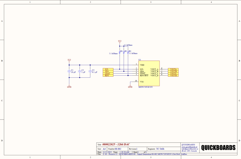
The MCP4728T utilizes a compact 10-pin footprint to provide four analog outputs and a high-speed digital interface. The mapping below outlines the connections utilized in this reference block.
| Pin Number | Primary Function | Secondary / Peripheral Functions |
| 1 | VDD | Positive Power Supply (3.3V) |
| 2 | SCL | I2C Serial Clock Input |
| 3 | SDA | I2C Serial Data Input/Output |
| 4 | LDAC | Latch DAC; Synchronous Update Input |
| 5 | RDY/BSY | Ready/Busy Status Output |
| 6 | VOUT_A | Analog Output Channel A |
| 7 | VOUT_B | Analog Output Channel B |
| 8 | VOUT_C | Analog Output Channel C |
| 9 | VOUT_D | Analog Output Channel D |
| 10 | VSS | Ground Reference (0V) |
Functional Block Analysis & Design Decisions
Tiered Decoupling Network
The schematic implements a tiered decoupling strategy using three ceramic capacitors: C1 (10uF), C2 (1uF), and C3 (0.1uF). In mixed-signal designs, a single capacitor is often insufficient to suppress noise across a wide frequency spectrum. The 0.1uF capacitor (C3) provides a low-impedance path to ground for high-frequency noise generated by the internal I2C logic switching. The 1uF (C2) and 10uF (C1) capacitors act as localized energy reservoirs to stabilize the 3.3V rail against lower-frequency transients caused by the quad-output buffers driving loads. These components should be placed in parallel as close to Pin 1 (VDD) as possible, with the smallest value (0.1uF) being the closest to the pin to minimize parasitic trace inductance.
I2C Pull-up and Control Resistors
Resistors R1, R2, and R3 are specified at 5.1 kOhms. For the SCL (Pin 2) and SDA (Pin 3) lines, these pull-up resistors define the inactive high state of the I2C bus. A value of 5.1 kOhms is a standard engineering compromise; it is low enough to ensure fast signal rise times (essential for 400kHz Fast-mode operation) while high enough to minimize static power consumption when the bus is pulled low. R3 serves as a pull-up for the LDAC (Pin 4) signal. By pulling LDAC high by default, the DAC outputs are updated as soon as their respective registers are written. If a synchronous update across all four channels is required, the host controller can pull this line low after all registers are populated.
Status and Ready Logic
Pin 5 (RDY/BSY) is a status indicator specifically used during EEPROM write cycles. When the device is busy writing new default power-up values to the internal non-volatile memory, this pin stays low. This design includes the net connection for this pin to allow the host processor to monitor the device status via polling or interrupt, preventing the overlapping of write commands which could lead to data corruption in the EEPROM.
Implementation Insights
When integrating this block into a larger PCB, analog signal integrity is paramount. Even though the MCP4728T provides rail-to-rail buffered outputs, the traces for VOUTA through VOUTD should be routed over a solid ground plane to minimize electromagnetic interference (EMI) pickup. It is advisable to maintain physical separation between these sensitive analog traces and the high-speed I2C digital traces (SCL/SDA) to prevent digital crosstalk from appearing as noise on the analog outputs.
The non-volatile memory feature requires careful software handling. While the EEPROM allows for convenient power-up states, it has a finite endurance (typically 1,000,000 erase/write cycles). Designers should ensure that the firmware only writes to the EEPROM when a persistent change is required, rather than for every dynamic output adjustment, to ensure long-term reliability of the module.
Applications
- Set Point or Offset Trimming: Automating the adjustment of analog voltage references or nulling offsets in precision sensor signal chains.
- Sensor Calibration: Providing variable compensation voltages to linearize or calibrate nonlinear sensor outputs in industrial environments.
- Mechanical Control: Driving precision actuators, servos, or valves where multiple coordinated analog control signals are required.
- Instrumentation: Multi-channel signal generation for automated test equipment (ATE) and laboratory power supplies.
Integrating the MCP4728T into your design
This modular reference block provides a pre-validated hardware foundation for quad-channel analog generation. By utilizing this block, engineers bypass the complexities of I2C bus termination and tiered power decoupling optimization. The layout-ready schematic ensures that the critical core support circuitry is correctly implemented, allowing teams to focus on application-level firmware and signal conditioning logic while reducing the risk of first-spin hardware failures.
Skip the tedious research and manual entry. Download the production-ready schematic block for the MCP4728T directly from the Quickboards Library.