AD1934WBSTZ-RL 24bit Digital to Analog Reference Schematic Design
The AD1934WBSTZ-RL is a high-performance, single-chip audio Digital-to-Analog Converter (DAC) that provides eight individual 24-bit outputs. Engineered for high-fidelity signal reproduction, it is a staple in automotive infotainment systems, professional audio equipment, and multi-channel home theater receivers. Its primary function is to translate high-resolution digital audio streams (up to 192 kHz) into clean, differential analog signals with a focus on high dynamic range and low distortion.
Unlock the Quickboards Library
Get instant access to this Altium Schematic and hundreds of other subcircuits. Hardware design, modularized. Schematic + Layout + Firmware. Built to IPC standards for zero re-spins.
Overview of the AD1934WBSTZ-RL
This IC utilizes a patented multibit sigma-delta architecture to minimize the effects of clock jitter and provide a robust signal-to-noise ratio. It features a flexible serial port that supports various data formats, including I2S and TDM, allowing it to interface seamlessly with modern Digital Signal Processors (DSPs). The integration of eight channels into a single 48-lead LQFP package allows for significant board space savings in multi-way active crossover systems and surround-sound applications.
| Feature | Specification |
| Resolution | 24-Bit |
| Number of Channels | 8 DAC Channels |
| Dynamic Range | 108 dB (unweighted) |
| Max Sample Rate | 192 kHz |
| THD + N | -94 dB |
| Operating Voltage | 3.3V (nominal) |
| Communication | SPI / I2C Control Port |
| Package | 48-Lead LQFP |
Pin Configuration and Function Mapping
The AD1934WBSTZ-RL requires precise interfacing between its high-speed digital clocking and sensitive analog outputs. The following table highlights the critical pin assignments utilized in this modular block.
| Pin Number | Primary Function | Secondary / Peripheral Functions |
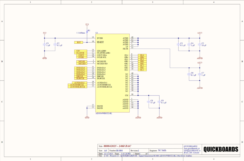
| 13 | DVDD | Digital Supply Voltage (3.3V) |
| 5, 33, 37, 48 | AVDD | Analog Supply Voltage (A3V3) |
| 1, 4, 32, 34, 36 | AGND | Analog Ground Reference |
| 12, 25 | DGND | Digital Ground Reference |
| 10 | PD/RST | Power-Down / Hardware Reset (Active Low) |
| 38 | CM | Common-Mode Reference Voltage |
| 35 | FILTR | Internal Filter / PLL Bypass Node |
| 2, 3 | MCLKI / MCLKO | Master Clock Input and Output |
| 23, 24, 26, 27 | Control Port | CIN, COUT, CCLK, CLATCH (SPI/I2C) |
| 28 – 31, 6 – 9 | OL / OR | Differential Analog Outputs (Left/Right 1-4) |
Functional Block Analysis & Design Decisions
Power and Decoupling Strategy
Audio fidelity is inextricably linked to power supply rejection. This design utilizes separate rails for digital (3V3) and analog (A3V3) supplies to prevent high-frequency digital switching transients from polluting the analog signal chain. The digital rail at pin 13 is decoupled with a 1uF (C1) and 0.1uF (C2) ceramic capacitor pair. For the analog rails (pins 5, 33, 37, 48), a tiered approach is employed: 0.1uF capacitors (C3, C4) are placed in immediate proximity to the pins to filter high-frequency noise, while a 10uF bulk capacitor (C5) provides a localized energy reservoir for low-frequency stability. Ceramic X7R dielectrics are specified for their low equivalent series resistance (ESR) and high stability over temperature.
Common-Mode Reference and Filtering
The Common-Mode (CM) pin (Pin 38) serves as the DC bias reference for the internal DAC stages. Any noise on this pin translates directly into the output signal, degrading the SNR. This design utilizes a high-capacitance 47uF electrolytic or high-density ceramic capacitor (C8) in parallel with a 0.1uF capacitor (C9) to ground. The 47uF value is critical for establishing an extremely low-frequency noise floor, while the 0.1uF capacitor handles high-frequency interference. Similarly, the FILTR node (Pin 35) is stabilized with a 1uF (C7) and 0.1uF (C6) network to ensure internal PLL stability and clean internal clock generation.
Output Signal Conditioning and Filtering
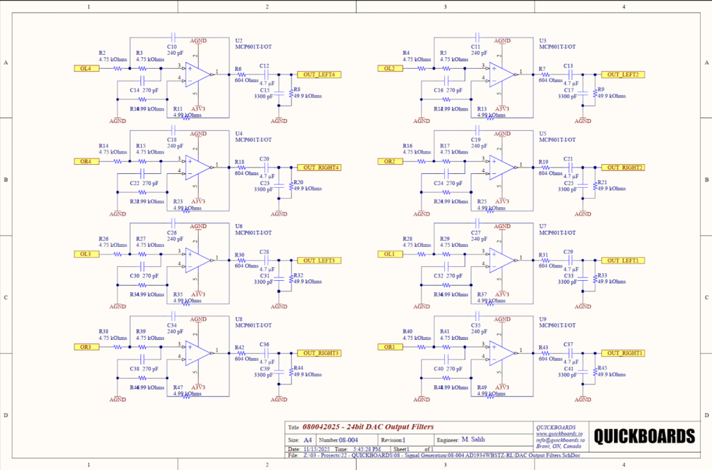
To remove high-frequency quantization noise and modulator artifacts, each of the eight analog outputs is routed through an active second-order low-pass filter. This design uses MCP601 op-amps in a multiple-feedback topology. Resistor choices such as 4.75k Ohms (R2, R3) and 4.99k Ohms (R11) are selected from the 1% E96 series to maintain gain matching across all eight channels—a prerequisite for balanced multi-channel audio. The capacitors (C10 at 240pF and C14 at 270pF) set the cutoff frequency. A final RC stage (604 Ohms and 4.7uF) provides DC blocking and impedance matching for the downstream stage, while R8 (49.9k) serves as a bleeder resistor to prevent DC pops during hot-plugging.
Hardware Control Logic
The Power-Down/Reset pin (Pin 10) is pulled high to the 3.3V digital rail via R1 (5.1k Ohms). This ensures that the device remains in an active state by default, preventing the DAC from entering an undefined power-down state if the control host is not yet initialized. The 5.1k Ohm value is a senior-level design choice that provides a robust pull-up strength to resist noise while remaining low enough in current to be easily overridden by a standard microcontroller GPIO for an intentional hardware reset.
Implementation Insights
A fundamental consideration when integrating this block is the master clock (MCLK) integrity. Given the 24-bit resolution, any jitter on the clock input at pins 2 and 3 will manifest as increased noise and distortion in the audio band. Traces for MCLK should be kept as short as possible, ideally routed over a continuous ground plane with controlled impedance.
Grounding is equally critical. To prevent digital return currents from flowing through the sensitive analog reference paths, a split ground plane strategy is recommended, where Analog Ground (AGND) and Digital Ground (DGND) are connected at a single “star point” near the power supply.
Users should be aware that the AD1934 defaults to a muted state on power-up. Firmware initialization must configure the control registers via SPI or I2C before audio will be produced. Additionally, ensure that the output op-amp (MCP601) rails are stable before unmuting the DAC to prevent transient audible “thumps” in the system.
Applications
- Automotive Infotainment: Used to drive multi-channel speaker arrays in premium vehicle head units and amplifiers.
- Professional Audio Interfaces: Implemented in studio-grade multi-channel interfaces for high-fidelity recording and playback.
- Home Theater Receivers: Serves as the primary conversion stage for 7.1 and 5.1 surround sound audio processing.
- Active Crossovers: Provides the necessary outputs for digital speaker management systems where each driver requires an independent, filtered analog signal.
Integrating the AD1934WBSTZ-RL into your design
This modular block provides a pre-validated hardware environment for high-resolution multi-channel conversion. By utilizing this sub-system, engineers eliminate the risks associated with common-mode reference noise and complex output filter tuning. The inclusion of high-precision resistor networks and optimized decoupling ensures that the AD1934 operates at its full theoretical dynamic range, reducing first-spin risk and allowing design teams to focus on high-level digital signal processing and system integration.
Skip the tedious research and manual entry. Download the production-ready schematic block for the AD1934WBSTZ-RL directly from the Quickboards Library.