MIC5158YM-TR Linear Regulator Reference Schematic Design
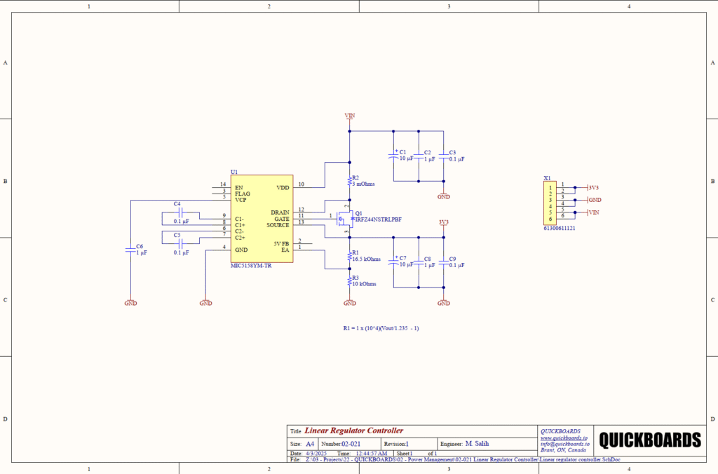
The MIC5158YM-TR is a “Super LDO” regulator controller designed to drive an external N-channel MOSFET pass element. This architecture allows for exceptionally low dropout voltages and high output currents, limited primarily by the characteristics of the chosen MOSFET rather than the controller itself. By utilizing an N-channel FET, which typically offers lower RDS(on) and cost compared to P-channel alternatives, this design achieves superior efficiency in high-current applications. It is commonly used in high-efficiency power supplies, battery chargers, and distributed power systems where minimal heat dissipation and maximum current delivery are required.
Unlock the Quickboards Library
Get instant access to this Altium Schematic and hundreds of other subcircuits. Hardware design, modularized. Schematic + Layout + Firmware. Built to IPC standards for zero re-spins.
Overview of the MIC5158YM-TR
The MIC5158 operates by using an internal charge pump to generate a gate drive voltage higher than the input supply, enabling the use of an N-channel MOSFET in a high-side configuration. This specific implementation provides a stable 3.3V output rail from a higher VIN source. The controller includes integrated current limiting, a low-battery/power-good flag, and an enable pin for system-level power sequencing.
| Feature | Specification |
| Input Voltage Range | 3V to 30V |
| Controller Type | N-Channel Linear Regulator Controller |
| Reference Voltage | 1.235V |
| Output Current | Limited by External MOSFET (e.g., 50A+) |
| Quiescent Current | 1mA (typical) |
| Shutdown Current | 10uA (typical) |
| Drive Type | Internal Charge Pump for N-FET |
| Protection | Current Limit and Thermal Shutdown |
Pin Configuration and Function Mapping
The MIC5158 is used in its 14-pin SOIC package to provide dedicated pins for the charge pump capacitors and error amplifier interfaces.
| Pin Number | Primary Function | Secondary / Peripheral Functions |
| 1 | EA | Error Amplifier Output |
| 2 | 5V FB | Feedback Input (for fixed 5V mode) |
| 3 | FLAG | Open-collector status output |
| 4 | GND | System Ground |
| 5 | VCP | Charge Pump Reservoir Capacitor |
| 6, 7 | C2-, C2+ | Charge Pump Capacitor 2 pins |
| 8, 9 | C1+, C1- | Charge Pump Capacitor 1 pins |
| 10 | VDD | Power Input for Controller |
| 11 | GATE | Gate Drive for External N-FET |
| 12 | DRAIN | Sense for Drain Voltage |
| 13 | SOURCE | Source Connection / Feedback Sense |
| 14 | EN | Logic Level Enable Input |
Functional Block Analysis & Design Decisions
Pass Element and Gate Drive
The design utilizes the IRFZ44NSTRLPBF, a robust N-channel MOSFET. An N-channel pass element is selected over a P-channel because N-channel devices offer significantly lower RDS(on) for the same silicon area, which is vital for high-current efficiency. Because the FET is on the high side, the GATE (Pin 11) must be driven several volts above VIN to fully enhance the channel. The MIC5158 handles this via its internal charge pump.
Charge Pump Network
Capacitors C4, C5 (0.1uF), and C6 (1uF) are required for the internal charge pump circuitry. These ceramic capacitors must be X7R or better to ensure stable capacitance over temperature and voltage. C4 and C5 act as the “flying” capacitors that transfer charge, while C6 acts as the reservoir for the VCP pin. The choice of 0.1uF for the flying capacitors is standard for the 100kHz to 500kHz internal switching frequency of the MIC5158.
Voltage Feedback and Accuracy
The output voltage is set to 3.3V using the resistor divider R1 (16.5 kOhms) and R3 (10 kOhms). The MIC5158 compares the voltage at the EA pin to an internal 1.235V reference. The value of R1 is determined by the formula R1 = R3 * (Vout / 1.235 – 1). Using 1% tolerance resistors is mandatory here to ensure the output remains within a tight regulation window, especially as the system temperature fluctuates.
Current Sensing and Overcurrent Protection
R2 is a 3 mOhm shunt resistor used for current sensing. The MIC5158 monitors the voltage drop across this resistor to protect the external MOSFET from overcurrent conditions. A value of 3 mOhms minimizes power dissipation (I squared * R) at high loads while providing a sufficient signal-to-noise ratio for the controller’s current limit comparator.
Input and Output Decoupling
Both input and output stages feature a triple-capacitor filter: 10uF electrolytic (C1, C7) for bulk storage, 1uF ceramic (C2, C8) for mid-frequency decoupling, and 0.1uF ceramic (C3, C9) for high-frequency noise suppression. This staggered approach is a standard requirement for high-performance linear regulators to ensure stability and low output ripple, particularly when the MOSFET is operating in its linear region.
Implementation Insights
Thermal management of the IRFZ44 MOSFET is the most critical system integration factor. Unlike a switching regulator, a linear regulator pass element dissipates power equal to the voltage drop across it multiplied by the load current (Vdiff * I). If dropping 5V to 3.3V at 10A, the FET must dissipate 17W. Sufficient heatsinking or large PCB copper pours are required to prevent thermal runaway.
For the current sense resistor R2, Kelvin connections (four-wire sensing) should be used in the PCB layout. High-current paths can create significant voltage drops on the PCB traces; if the sense lines are not connected directly to the resistor pads, the current limit may trigger prematurely or inconsistently.
Applications
- High Current Post-Regulators: Used to clean up the output of a switching regulator while maintaining high current capability for sensitive digital loads.
- Battery Chargers: Providing a controlled constant-voltage, constant-current charging profile for large lead-acid or lithium-ion banks.
- Distributed Power Systems: Locally regulating power rails in industrial racks where low noise and high reliability are paramount.
- Automotive Power Modules: Managing high-current 12V or 24V subsystems that require low dropout during cold-crank conditions.
Integrating the MIC5158YM-TR into your design
This modular schematic block provides a pre-validated high-current linear regulation stage that overcomes the current limitations of integrated LDOs. By using an external N-channel pass element and a sophisticated gate drive controller, the design ensures maximum efficiency and stability. This sub-system is ready for integration into larger power trees, providing a clean, high-current output with minimal external design complexity.
Skip the tedious research and manual entry. Download the production-ready schematic block for the MIC5158YM-TR directly from the Quickboards Library.