MCP3564R 24bit Analog to Digital Converter Reference Schematic Design
The MCP3564R is a high-performance, 24-bit Delta-Sigma Analog-to-Digital Converter (ADC) from Microchip, engineered for high-precision measurement applications. Featuring a programmable data rate up to 153.6 ksps and an integrated 20 ppm/Celsius internal voltage reference, it provides a sophisticated solution for digitizing low-level analog signals. This device is typically utilized in precision instrumentation, industrial process control, and high-accuracy sensor interfaces where signal-to-noise ratio and linearity are paramount.
Unlock the Quickboards Library
Get instant access to this Altium Schematic and hundreds of other subcircuits. Hardware design, modularized. Schematic + Layout + Firmware. Built to IPC standards for zero re-spins.
Overview of the MCP3564R
This IC utilizes a Delta-Sigma architecture to achieve high resolution by oversampling the input signal and performing noise shaping. By shifting quantization noise into higher frequencies and then applying digital filtering, the MCP3564R can resolve signals that would be lost in the noise floor of standard SAR-based converters. Its multi-channel multiplexer allows for up to 8 differential or 16 single-ended channels, making it a versatile hub for complex sensor arrays.
| Feature | Specification |
| Resolution | 24-bit |
| Architecture | Delta-Sigma |
| Max Data Rate | 153.6 ksps |
| Input Channels | 8 Differential / 16 Single-Ended |
| Internal Reference | 2.4V (20 ppm/Celsius) |
| Interface | 20 MHz SPI |
| Operating Voltage | 2.7V to 3.6V (AVDD/DVDD) |
| Package | 20-lead TSSOP |
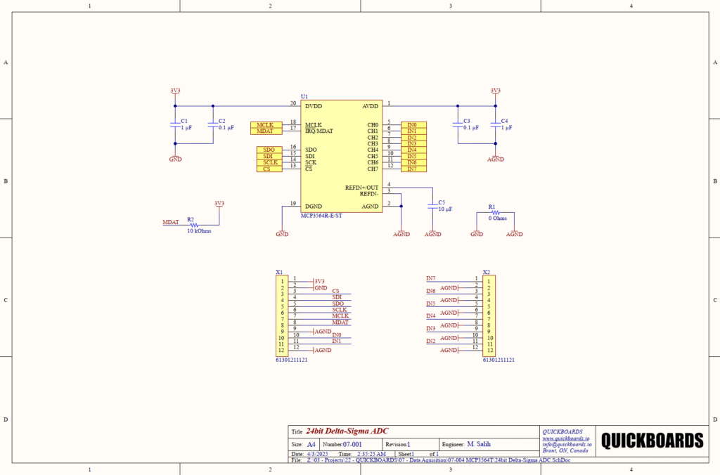
Pin Configuration and Function Mapping
The MCP3564R in its 20-lead TSSOP package provides a streamlined interface for both high-speed digital communication and sensitive analog sampling.
| Pin Number | Primary Function | Secondary / Peripheral Functions |
| 1 | AVDD | Analog Power Supply Input |
| 2 | AGND | Analog Ground Reference |
| 3 | REFIN- | Negative Reference Input |
| 4 | REFIN+/OUT | Positive Reference Input or Internal Ref Output |
| 5 – 12 | CH0 – CH7 | Analog Input Channels (Multiplexed) |
| 13 | CS | SPI Chip Select (Active Low) |
| 14 | SCK | SPI Serial Clock Input |
| 15 | SDI | SPI Serial Data Input |
| 16 | SDO | SPI Serial Data Output |
| 17 | IRQ/MDAT | Interrupt Request or Modulator Data Output |
| 18 | MCLK | External Master Clock Input |
| 19 | DGND | Digital Ground Reference |
| 20 | DVDD | Digital Power Supply Input |
Functional Block Analysis & Design Decisions
Power and Decoupling Strategy
The schematic implements a strict separation between the Analog Supply (AVDD) and the Digital Supply (DVDD). While both are connected to the 3.3V rail (3V3), they are decoupled independently to prevent digital switching noise from the ADC core and SPI bus from coupling into the sensitive analog front-end. Each supply pin is supported by a 1uF (C1, C4) and 0.1uF (C2, C3) ceramic capacitor pair. The 0.1uF capacitors are selected for their low equivalent series inductance (ESL) to handle high-frequency transients, while the 1uF capacitors act as localized energy reservoirs for lower-frequency ripple. For 24-bit precision, these must be placed as close as possible to the IC pins to minimize trace inductance, which can degrade the noise floor of the converter.
Voltage Reference Stabilization
The MCP3564R features an internal voltage reference available at the REFIN+/OUT pin. To ensure the stability of this reference during the charge-redistribution phase of the conversion, a 10uF capacitor (C5) is connected between the reference pins. This high-value ceramic capacitor suppresses voltage droop when the internal sampling capacitors switch, which is essential for maintaining absolute gain accuracy. Ceramic X7R or X5R types are chosen here for their stability over temperature and voltage, as the reference stability directly dictates the precision of the conversion result.
Grounding and Noise Mitigation
A critical design choice in this block is the implementation of R1, a 0 Ohm resistor acting as a “net-tie” between Digital Ground (GND) and Analog Ground (AGND). This ensures that while the grounds are separate on the PCB to isolate return paths, they are tied at a single star-point to prevent potential differences that could lead to measurement errors. Furthermore, R2 (10 kOhms) is used as a pull-up on the MDAT line to 3.3V, defining a default state for the interrupt/data line and preventing it from floating when the output is in a high-impedance state.
Interface and Clocking
The digital interface is broken out through connector X1, providing access to the SPI bus and the Master Clock (MCLK). Utilizing an external MCLK allows the ADC to be synchronized with a host processor’s timing, which is vital for reducing phase jitter in time-sensitive measurements. The analog inputs (CH0-CH7) are grouped on connector X2, with interleaved AGND pins to provide clear return paths and minimize crosstalk between adjacent channels during high-speed scanning.
Implementation Insights
Precision 24-bit designs are highly susceptible to electromagnetic interference and thermal gradients. When integrating this block, ensure that the analog input traces are routed differentially where possible and kept far from the high-speed SPI clock lines. Even small amounts of digital crosstalk can manifest as periodic noise in the converted data.
Potential integration risks include neglecting the drive capability of the analog source. Because Delta-Sigma ADCs utilize a switched-capacitor input stage, they present a dynamic load to the sensor or buffer amplifier. If the source impedance is too high, the input will not settle within the sampling window, leading to significant non-linearity. Utilizing a low-noise, high-bandwidth operational amplifier as an input buffer is standard practice for maintaining full 24-bit performance.
Another risk involves the layout of the VCAP/VREF path. If the 10uF stabilization capacitor is placed far from the IC, the resulting parasitic resistance can increase the internal noise of the reference, effectively reducing the Effective Number of Bits (ENOB) to 16 or 18.
Applications
- Weight Scales and Force Sensors: High resolution allows for the detection of minute changes in load cell outputs without the need for high-gain analog pre-amplification.
- Temperature Controllers: Interfaces directly with RTDs and thermocouples, utilizing the internal gain stages to resolve millivolt-level signals.
- Industrial Pressure Transmitters: Provides robust digitization in noisy environments through differential signaling and digital filtering.
- Precision Medical Instrumentation: Suitable for diagnostic equipment requiring high dynamic range and low power consumption for portable operation.
Integrating the MCP3564R into your design
This modular block provides a pre-validated hardware foundation for 24-bit data acquisition, managing the complexities of supply isolation and reference stabilization. By utilizing this sub-system, designers can eliminate the repetitive tasks of reference circuitry optimization and grounding strategy definition. This allows your team to focus on digital signal processing and application-level logic while ensuring the hardware remains capable of achieving the highest possible signal integrity.
Skip the tedious research and manual entry. Download the production-ready schematic block for the MCP3564R directly from the Quickboards Library.