PIC16F872T Reference Schematic Design
Developing a standardized, reusable schematic block for the PIC16F872T allows hardware teams to accelerate the prototyping phase while maintaining high signal integrity and power stability. This processor block is engineered to serve as a reliable “drop-in” core for 8-bit embedded systems, ensuring that critical timing and programming interfaces are validated before the first PCB spin.
Unlock the Quickboards Library
Get instant access to this Altium Schematic and hundreds of other subcircuits. Hardware design, modularized. Schematic + Layout + Firmware. Built to IPC standards for zero re-spins.
Overview of the PIC16F872T
The PIC16F872T is a high-performance RISC microcontroller from Microchip, designed for applications that require a balance of analog integration and low power consumption. It is frequently employed in industrial sensor nodes, handheld medical devices, and automotive subsystems. Its ability to execute most instructions in a single cycle makes it a highly efficient choice for real-time control logic.
Technical Specification
| Feature | Value / Feature |
| Operating Voltage | 2.0V to 5.5V |
| Architecture | 8-bit RISC |
| Flash Program Memory | 3.5 KB |
| RAM / EEPROM | 128 Bytes / 64 Bytes |
| Max Operating Frequency | 20 MHz |
| ADC Resolution | 10-bit (5 Channels) |
| Communication | I2C, SPI, UART |
| Package Type | 28-pin SSOP/SOIC |
Pin Configuration and Function Mapping
To ensure the block is easily adaptable, the following functional mapping is utilized in the schematic design. Understanding these multiplexed pins is essential for selecting appropriate peripheral assignments in the firmware.
| Pin Number | Primary Function | Secondary / Peripheral Function |
| 1 | MCLR/VPP | Master Clear / Programming Voltage |
| 2–5 | RA0–RA3 | Analog Inputs (AN0–AN3) / VREF |
| 9, 10 | OSC1, OSC2 | External Crystal Input / Output |
| 11–18 | RC0–RC7 | Timers, I2C (SDA/SCL), UART (TX/RX) |
| 21–28 | RB0–RB7 | External Interrupts, ICSP (PGC/PGD) |
Functional Block Analysis & Design Decisions
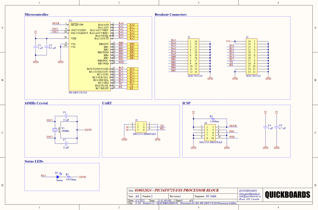
Examination of the PIC16F872T processor block reveals several critical sub-circuits designed for maximum stability and production-grade reliability.
Power Supply & Decoupling
The schematic utilizes a dual-capacitor decoupling strategy for the VDD (Pin 20) rail.
- Component Selection: A 1 uF (C1) and a 0.1 uF (C2) ceramic capacitor are placed in parallel. The 0.1 uF capacitor is a high-frequency bypass intended to suppress digital switching noise, while the 1 uF capacitor provides local bulk storage to prevent voltage dips during transient loads. Ceramic X7R types are preferred here for their temperature stability.
- Placement & Trace Logic: These must be placed as close to the VDD and VSS pins as possible. Minimizing the trace length reduces parasitic inductance, which is vital for the capacitors to effectively filter high-frequency transients.
Timing & Oscillation
To provide a stable clock for the CPU and baud-rate generation, a 16MHz Crystal (Y1) circuit is implemented.
- Component Selection: The crystal is paired with two 22 pF (C3, C7) load capacitors. These values are selected to match the typical load capacitance (CL) requirements of an HC-49 or SMD crystal, ensuring the oscillator starts reliably and remains within frequency tolerances.
- Design Rationale: While the PIC can run on an internal RC oscillator, an external crystal is mandatory for applications requiring precise timing, such as UART communication or synchronized industrial bus protocols.
Programming Interface (ICSP)
The In-Circuit Serial Programming (ICSP) block allows for firmware updates without removing the IC from the PCB.
- Design Rationale: The MCLR (Pin 1) is tied to a 1 kOhm resistor (R1) pull-up. This resistor serves dual purposes: it prevents the MCU from entering a random reset state due to EMI and acts as a current limiter when the programmer applies a high voltage (VPP) to the pin.
- Protection: The inclusion of bulk capacitance (C4, C8) on the programming header’s power rail ensures that the voltage remains stable during the high-current flash-writing process.
Status Indication & Connectivity
- Visual Feedback: A green LED (D1) is connected to RA5 through a 470 Ohm resistor (R2). This resistor limits the current to approximately 6.5mA, ensuring the LED is bright enough for diagnostic use while remaining well below the IC’s maximum GPIO source current.
- Breakout Connectors: High-density headers (J1, J2) provide access to all GPIOs. The layout logic here implies the use of interleaved ground pins to maintain signal integrity when connecting via ribbon cables or jumpers.
Thermal and Power Management
The PIC16F872T is a low-power device, but thermal management remains a factor in high-density designs or when driving multiple LEDs.
- Thermal Dissipation: In the SSOP package, heat is primarily dissipated through the ground pins. The schematic connects Pins 8 and 19 (VSS) to a common ground plane, which acts as a heat sink to maintain a low junction temperature.
- Current Budgeting: The status LED (D1) on RA5 is limited by a 470 Ohm resistor (R2), drawing approximately 6.5mA. This ensures the total source current of the RA port remains well within the safe operating area of the silicon, preventing localized hotspots within the IC.
Implementation Insights for Engineers
- ADC Reference Stability: For designs utilizing the 10-bit ADC, the accuracy is directly proportional to the stability of the voltage on VDD. If high precision is required, it is advisable to use a dedicated voltage reference on Pin 5 (VREF+), isolated from the digital VDD rail via a ferrite bead.
- Unused Port Termination: Any GPIO pins not utilized in the final application should be configured as outputs and driven to a static logic level (Low) in software. This prevents the CMOS input stages from oscillating and drawing unnecessary current.
- Clock Path Routing: When laying out the PCB for this block, keep the OSC1 and OSC2 traces symmetrical and as short as possible. Avoid routing high-speed digital lines (like UART TX/RX) directly underneath the crystal to prevent capacitive coupling and clock jitter showing on the UART bus.
Applications
The PIC16F872T is engineered for versatility in low-power, cost-sensitive environments where analog-to-digital conversion and deterministic control are required. Its robust 8-bit architecture and integrated EEPROM make it a “set-and-forget” solution for various industrial and consumer sectors.
Typical applications for this microcontroller include:
- Industrial Process Control: Used in PLC (Programmable Logic Controller) expansion modules, dedicated PID temperature controllers, and fluid level monitoring systems.
- Automotive Subsystems: Ideal for secondary body electronics, such as power window controllers, side-mirror adjustment logic, and interior lighting dimming modules.
- Smart Sensor Nodes: Often used as an interface bridge for analog sensors (pressure, humidity, or strain gauges), converting signals to digital data for transmission over I2C or SPI buses.
- Consumer Appliances: Integrated into small household electronics like digital thermostats, coffee machine logic controllers, and battery charging stations.
- Handheld Medical Devices: Its low-power “Sleep” mode makes it suitable for portable diagnostic equipment, such as digital pulse oximeters or glucose meters.
- Legacy Logic Replacement: A high-reliability choice for modernizing older hardware designs that previously relied on discrete logic gates or older 8051-based architectures.
Integrating the PIC16F872T into Your Design
By utilizing this validated processor block, the fundamental hardware challenges—such as oscillator start-up, power sequencing, and programming interface reliability—are resolved out of the box. This modular approach allows engineering teams to focus on the higher-level application logic and peripheral integration, ensuring a faster path to a functional first-spin prototype.
Skip the tedious research and manual entry. Download the production-ready schematic block for the PIC16F872T directly from the Quickboards Library.