MTS62C19A-HS105 Dual Full-Bridge Stepper Motor Driver Reference Schematic Design
Overview of the MTS62C19A-HS105
The MTS62C19A-HS105 is a high-performance dual full-bridge motor driver designed to control both windings of a bipolar stepper motor or bidirectionally control two DC motors. This integrated circuit incorporates internal PWM current control and power MOSFETs capable of handling significant loads, making it a staple in precision motion control systems. Its primary function is to translate low-level logic signals into the high-power drive sequences required for inductive loads.
Unlock the Quickboards Library
Get instant access to this Altium Schematic and hundreds of other subcircuits. Hardware design, modularized. Schematic + Layout + Firmware. Built to IPC standards for zero re-spins.
Typically, this IC is found in applications where board space and reliability are paramount, such as office automation, medical instrumentation, and small-scale robotics. By integrating the power stage and control logic, it reduces the complexity of the external drive circuitry significantly.
| Technical Specification | Value |
| Load Supply Voltage (VLOAD) | 10V to 30V |
| Logic Supply Voltage (VLOGIC) | 4.75V to 5.25V |
| Output Current (Continuous) | Up to 1.0A |
| Control Methodology | Internal PWM Current Control |
| Input Logic Levels | TTL / CMOS Compatible (5V) |
| Protection Features | Thermal Shutdown and Undervoltage Lockout |
| Package Type | HSOP-20 / SOP-24 (Design dependent) |
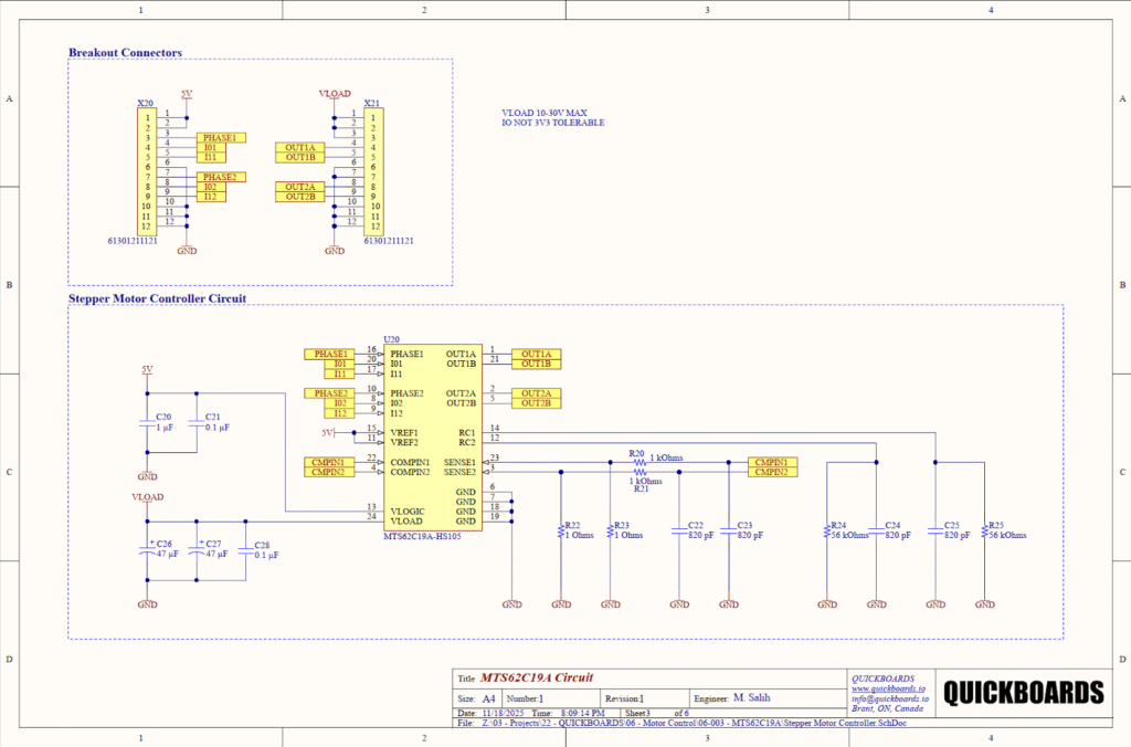
Pin Configuration and Function Mapping
The MTS62C19A-HS105 utilizes a high-pin-count architecture to separate sensitive analog feedback from high-current motor outputs. The following table maps the pins as utilized in this reference design.
| Pin Number | Primary Function | Secondary / Peripheral Function |
| 1 | OUT1A | Bridge 1 Output A |
| 2 | OUT2A | Bridge 2 Output A |
| 3 | SENSE2 | Bridge 2 Current Sense Input |
| 4 | COMPIN2 | Bridge 2 Comparator Input |
| 5 | OUT2B | Bridge 2 Output B |
| 6, 7 | GND | Power Ground |
| 8 | I02 | Bridge 2 Current Logic Input (LSB) |
| 9 | I12 | Bridge 2 Current Logic Input (MSB) |
| 10 | PHASE2 | Bridge 2 Direction Control |
| 11 | VREF2 | Bridge 2 Reference Voltage |
| 12 | RC2 | Bridge 2 PWM Off-Time Timing |
| 13 | VLOGIC | 5V Logic Supply |
| 14 | RC1 | Bridge 1 PWM Off-Time Timing |
| 15 | VREF1 | Bridge 1 Reference Voltage |
| 16 | PHASE1 | Bridge 1 Direction Control |
| 17 | I11 | Bridge 1 Current Logic Input (MSB) |
| 18, 19 | GND | Power Ground |
| 20 | I01 | Bridge 1 Current Logic Input (LSB) |
| 21 | OUT1B | Bridge 1 Output B |
| 22 | COMPIN1 | Bridge 1 Comparator Input |
| 23 | SENSE1 | Bridge 1 Current Sense Input |
| 24 | VLOAD | Motor Load Supply (10-30V) |
Functional Block Analysis & Design Decisions
The design of this motor controller block is centered on stability and noise immunity, which are critical when dealing with the high-frequency switching of inductive loads.
Power and Decoupling Strategy
The schematic implements separate decoupling strategies for the logic (5V) and load (VLOAD) rails. For VLOGIC, a combination of C20 (1 uF) and C21 (0.1 uF) ceramic capacitors is used. The 0.1 uF capacitor handles high-frequency transients, while the 1 uF provides a local reservoir for switching logic. On the VLOAD rail, the design utilizes a high-capacitance bulk decoupling stage consisting of two 47 uF capacitors (C26, C27) in parallel with a 0.1 uF ceramic capacitor (C28). The bulk capacitance is essential to absorb the back-EMF and current spikes generated by the motor coils, preventing voltage sagging or spikes that could reset the IC. These components must be placed as close as possible to pins 13 and 24 to minimize trace inductance.
Timing and PWM Control (RC Networks)
The PWM “off-time” is determined by external RC networks on pins 12 and 14. In this design, R24/R25 (56 kOhms) and C24/C25 (820 pF) are selected to define the frequency of the internal fixed-off-time PWM regulator. This selection ensures the switching frequency remains outside the audible range while maintaining efficiency. Using 1% tolerance resistors and COG/NP0 type capacitors is recommended here to ensure the timing remains consistent across temperature variations, preventing “beat frequencies” or resonance in the motor.
Current Sensing and Signal Conditioning
Current sensing is achieved via R22 and R23 (1 Ohm resistors) connected between the SENSE pins and ground. A 1 Ohm value provides a direct 1:1 voltage-to-current ratio for the internal comparator, simplifying firmware development. However, the raw signal at the sense resistor is often noisy due to MOSFET switching. To mitigate this, a low-pass filter (Signal Conditioning block) is implemented using R20/R21 (1 kOhm) and C22/C23 (820 pF) before the signal reaches the COMPIN pins. This RC filter prevents the PWM logic from being prematurely tripped by “ringing” or leading-edge current spikes when the bridge switches.
Implementation Insights
A critical consideration for the MTS62C19A-HS105 is its logic level sensitivity. As noted in the design, the IO pins are not 3.3V tolerant; they require a strict 5V logic environment. If integrating this with a 3.3V microcontroller (such as an ESP32 or STM32), level shifters must be implemented on the PHASE and I-logic lines to ensure reliable switching and prevent damage to the IC’s input stages.
Thermal management is another vital engineering factor. The GND pins (6, 7, 18, 19) serve as the primary thermal path for the internal power bridges. These should be connected to a large, unbroken ground plane on the PCB. In high-duty-cycle applications, adding thermal vias to a bottom-layer copper pour will significantly reduce junction temperature and prevent the internal thermal shutdown from triggering during operation.
Proper grounding of the sense resistors (R22, R23) is paramount. These should have a dedicated, short path to the power ground pins of the IC to avoid ground loops. Any parasitic resistance in the ground path between the sense resistor and the IC will be interpreted as additional motor current, leading to reduced torque and unpredictable motor behavior.
Applications
- Office Automation: Used in printers and scanners for precise carriage movement and paper feed control where low noise and high reliability are required.
- 3D Printing: Provides the necessary drive current for NEMA 17 or smaller bipolar motors used in consumer-grade additive manufacturing.
- Medical Equipment: Ideal for peristaltic pumps and automated laboratory equipment requiring smooth, jitter-free motion.
- Industrial Controls: Employed in small-scale valve actuators and positioners within automated factory environments.
Integrating the MTS62C19A-HS105 into your design
The MTS62C19A-HS105 modular block simplifies the design process by providing a pre-validated environment for current sensing and PWM timing. By utilizing this proven sub-circuit, engineers can focus on high-level system logic rather than the intricacies of motor-driver stability and noise suppression.
Skip the tedious research and manual entry. Download the production-ready schematic block for the MTS62C19A-HS105 directly from the Quickboards Library.