ACS711KEXLT-15AB-T 15A Current Sensor Reference Schematic Design
The ACS711KEXLT-15AB-T is a Hall effect-based linear current sensor IC designed for low-side or high-side current sensing in AC or DC systems. Unlike traditional shunt-based measurement systems, this device utilizes an integrated, low-resistance copper conduction path. As current flows through this internal path, it generates a magnetic field that is sensed by the integrated Hall IC and converted into a proportional voltage. This architecture provides a compact, cost-effective solution for overcurrent protection and monitoring in space-constrained applications such as motor control, load management, and switched-mode power supplies.
Unlock the Quickboards Library
Get instant access to this Altium Schematic and hundreds of other subcircuits. Hardware design, modularized. Schematic + Layout + Firmware. Built to IPC standards for zero re-spins.
Typical applications include phase current monitoring in small motors, battery management systems (BMS), and power distribution units where precise current tracking is required without the thermal overhead or board space consumption of bulky external shunt resistors.
| Technical Specification | Details |
| Supply Voltage (VCC) | 3.0V to 5.5V |
| Full-Scale Current Range | +/- 15.5A |
| Sensitivity | 90 mV/A (at VCC = 3.3V) |
| Internal Conductor Resistance | 0.6 mOhm |
| Operating Temperature | -40 to 125 Celsius |
| Overcurrent Fault Trip Point | 100 percent of Full-Scale |
| Response Time | 4.6 microseconds |
| Output Type | Ratiometric Analog Voltage |
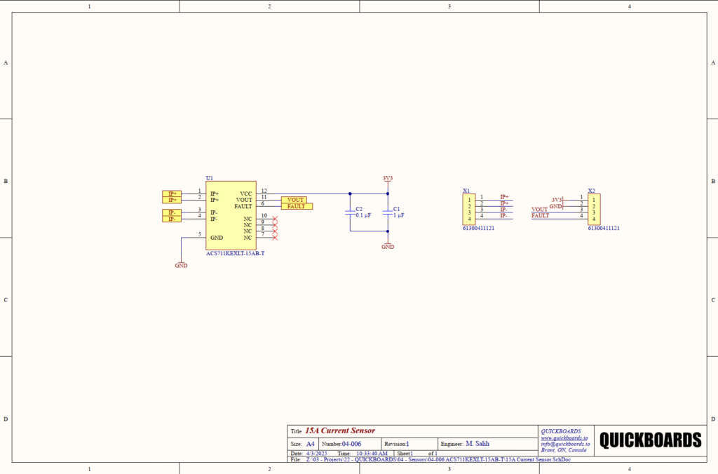
Pin Configuration and Function Mapping
The ACS711 is housed in a low-profile EX package (QFN). The pinout is strategically arranged to separate the high-current primary path from the sensitive low-power signal pins.
| Pin Number | Primary Function | Secondary / Peripheral Functions |
| 1, 2 | IP+ | Terminals for current being sensed |
| 3, 4 | IP- | Terminals for current being sensed |
| 5 | GND | Device Ground reference |
| 6 | FAULT | Active-low overcurrent fault output |
| 7, 8, 9, 10 | NC | No internal connection |
| 11 | VOUT | Analog output proportional to current |
| 12 | VCC | Device Power Supply |
Functional Block Analysis & Design Decisions
Power and Decoupling Strategy
The power sub-circuit focuses on Pin 12 (VCC). For Hall effect sensors, supply stability is paramount because the output voltage is ratiometric to the input voltage. This design utilizes a dual-capacitor decoupling scheme consisting of C1 (1 uF) and C2 (0.1 uF). The 0.1 uF capacitor is a high-frequency bypass component chosen for its low equivalent series inductance (ESL) to filter out high-frequency switching noise from nearby digital logic. The 1 uF capacitor acts as a localized bulk reservoir to stabilize the supply against lower-frequency transients. Both capacitors are specified as Ceramic X7R types, as these provide superior temperature stability and a lower voltage coefficient compared to Y5V or electrolytic alternatives.
Primary Current Path (IP+ / IP-)
The high-current path is handled through Pins 1, 2, 3, and 4. The internal resistance of this path is exceptionally low at 0.6 mOhm, which minimizes power dissipation and self-heating at the 15A rating. In the schematic, these pins are broken out to the X1 connector. To ensure the rated accuracy and prevent PCB delamination at high currents, these traces must be designed with significant copper weight (e.g., 2 oz or higher) and wide geometry. The grouping of pins 1-2 and 3-4 effectively parallelizes the connection to reduce contact resistance and spread thermal load across the IC leadframe.
Signal Conditioning and Fault Indication
The measurement block consists of the VOUT (Pin 11) and FAULT (Pin 6) signals. VOUT provides the analog representation of the current, centered at VCC / 2 for zero-current flow. Pin 6 is an open-drain FAULT output that transitions low when the sensed current exceeds the device’s full-scale limit. While this schematic provides the raw signal path, a pull-up resistor (typically 10 kOhms) is required on the host-side logic to define the high state. This allows for rapid overcurrent detection independent of the microcontroller’s ADC sampling rate.
Placement & Trace Logic
The physical layout requirements for this block are driven by thermal management and magnetic integrity. The decoupling capacitors C1 and C2 must be placed within 2mm of Pin 12 to ensure the noise-filtering remains effective. For the current path, traces should be routed symmetrically into the IP pins. Senior engineers should ensure that no high-current return paths or high-speed switching signals are routed directly beneath the ACS711, as external magnetic fields can interfere with the Hall effect element and induce measurement errors.
Implementation Insights
A critical consideration when integrating the ACS711 is the ratiometric nature of the output. Because VOUT is relative to VCC, any noise or drift on the 3.3V rail will translate directly into a measurement error. If the host ADC uses a different reference voltage than the ACS711 supply, a software-based compensation or a shared reference voltage should be used to maintain accuracy.
Thermal management of the PCB is the second high-level consideration. At 15A continuous current, the 0.6 mOhm internal resistance generates approximately 0.135 Watts. While this is low, the small QFN package relies on the PCB traces as its primary heat sink. Increasing the area of the copper pours connected to Pins 1-4 is essential to keep the junction temperature within the safe operating area during prolonged high-load conditions.
Finally, internal shielding on the ACS711 provides immunity to stray electric fields, but it remains susceptible to stray magnetic fields. In high-density power designs, placing the sensor away from large inductors or transformers is necessary to prevent magnetic coupling that could be misinterpreted as measured current.
Applications
- Motor Phase Current Sensing: Monitoring the individual phase currents in brushless DC (BLDC) motors for commutation and torque control.
- Overcurrent Protection: Providing a fast hardware-level interrupt via the FAULT pin to shut down power stages during short-circuit events.
- Battery Discharge Monitoring: Tracking current consumption in portable power tools or light electric vehicles to estimate remaining state-of-charge.
- Server Power Management: Real-time power usage monitoring in high-density rack servers to optimize cooling and power distribution.
Integrating the ACS711KEXLT-15AB-T into your design
This modular reference block provides a pre-validated, production-ready footprint and support circuitry for the ACS711 current sensor. By utilizing the specific decoupling values and standardized current path mapping provided here, engineers can skip the tedious evaluation of supply stability and move directly to system-level integration. This block eliminates the typical uncertainty associated with Hall effect sensor implementation, specifically regarding power integrity and fault handling, resulting in a more predictable hardware outcome.
Skip the tedious research and manual entry. Download the production-ready schematic block for the ACS711KEXLT-15AB-T directly from the Quickboards Library.