LM75BDP-118 Digital Temperature Sensor Reference Schematic Design
The LM75BDP-118 is an industry-standard digital temperature sensor that integrates a high-precision Delta-Sigma analog-to-digital converter (ADC) and an I2C communication interface. Its primary function is to provide highly accurate ambient temperature data to a host controller while offering a programmable overtemperature shutdown output (OS). This IC is a staple in system thermal management, used to monitor critical components such as processors, memory modules, and power supplies. By providing a digital output, it eliminates the noise susceptibility issues associated with analog thermistor strings, making it ideal for complex, high-density electronic assemblies.
Unlock the Quickboards Library
Get instant access to this Altium Schematic and hundreds of other subcircuits. Hardware design, modularized. Schematic + Layout + Firmware. Built to IPC standards for zero re-spins.
Overview of the LM75BDP-118
The device operates over a wide temperature range of -55 degrees Celsius to +125 degrees Celsius. It features a programmable temperature threshold and hysteresis, allowing it to function as a standalone thermostat. The LM75BDP-118 is particularly valued for its low power consumption and its ability to support up to eight different devices on a single I2C bus through hardware address pins.
| Technical Specification | Value |
| Supply Voltage Range | 2.8V to 5.5V |
| Temperature Accuracy | +/- 2 degrees Celsius (typical) |
| Resolution | 11-bit (0.125 degrees Celsius per LSB) |
| Interface Type | I2C / SMBus |
| Bus Frequency | Up to 400 kHz |
| Supply Current | 280 microamps (typical) |
| Shutdown Current | 3.5 microamps (typical) |
| Package Type | TSSOP8 |
Pin Configuration and Function Mapping
The LM75BDP-118 utilizes a standard TSSOP8 footprint, providing a compact solution for high-density PCB designs.
| Pin Number | Primary Function | Secondary / Peripheral Functions |
| 1 | SDA | I2C Serial Data Input/Output |
| 2 | SCL | I2C Serial Clock Input |
| 3 | OS | Overtemperature Shutdown Output (Open-Drain) |
| 4 | GND | System Ground |
| 5 | A2 | User-defined I2C Address Bit 2 |
| 6 | A1 | User-defined I2C Address Bit 1 |
| 7 | A0 | User-defined I2C Address Bit 0 |
| 8 | VCC | Positive Power Supply (3.3V) |
Functional Block Analysis & Design Decisions
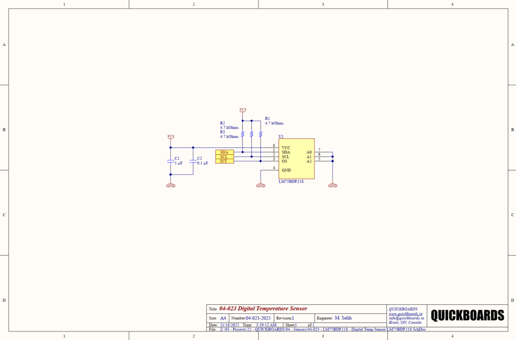
Power and Decoupling Block
The power sub-circuit for the LM75BDP-118 focuses on Pin 8 (VCC), which is connected to the 3.3V system rail. To ensure the integrity of the internal Delta-Sigma ADC, the design employs a dual-capacitor decoupling strategy using C1 (1 microfarad) and C2 (0.1 microfarad). The 0.1 microfarad capacitor is a high-frequency bypass component, selected for its low equivalent series inductance (ESL) to filter out fast switching transients from nearby digital logic. The 1 microfarad capacitor serves as a bulk reservoir to stabilize the supply during the sensor’s conversion cycles. Ceramic X7R capacitors are used here due to their excellent temperature stability and low aging rates, which are critical for maintaining ADC accuracy over the sensor’s long lifecycle.
Communication and Addressing Interface
Digital communication is handled via the I2C interface on Pins 1 and 2. This reference block utilizes 4.7 kOhm pull-up resistors (R2 and R3) on the SDA and SCL lines. A resistance of 4.7 kOhms is the industry standard for 400 kHz Fast-mode I2C operation; it provides a sufficiently fast rise time to meet timing specifications while minimizing static power consumption when the bus is pulled low. Pins 5, 6, and 7 (A2, A1, A0) are tied directly to GND. This hardware configuration hard-codes the I2C slave address to 1001000b (0x48). Tying these pins directly to ground rather than leaving them floating ensures bus stability and prevents address “ghosting” caused by electromagnetic interference.
Interrupt and Signal Conditioning
The OS (Overtemperature Shutdown) pin at Pin 3 is configured as a dedicated interrupt or watchdog output. Because this pin is an open-drain architecture, it requires a pull-up resistor to define the “High” state. R1 (4.7 kOhms) is used to pull the OS line to the 3.3V rail. This design rationale allows the OS pin to be used in a wired-OR configuration with other sensors if necessary. The OS pin can be programmed in firmware to trigger a hardware shutdown or a system interrupt when the temperature exceeds a user-defined setpoint, providing a critical safety layer that functions independently of the host microcontroller’s polling rate.
Implementation Insights
A primary engineering consideration for the LM75BDP-118 is the thermal path. Since the sensor measures its own die temperature, the PCB layout must facilitate thermal conduction between the target heat source and the IC package. Senior engineers should utilize a solid ground plane and, if possible, thermal vias near the GND pin (Pin 4) to improve thermal coupling to the board.
Self-heating is another factor to consider. Although the IC consumes very little power, continuous high-speed I2C communication can cause a slight temperature rise within the package, potentially skewing the ambient readings by a fraction of a degree. In precision applications, it is advisable to use the software shutdown mode between readings to minimize power dissipation.
Trace logic for the I2C bus should be designed with bus capacitance in mind. If this modular block is placed far from the host controller, the 4.7 kOhm pull-up resistors may need to be adjusted downward to 2.2 kOhms to maintain signal integrity against increased trace capacitance.
Applications
- System Thermal Management: Monitoring the internal temperature of high-performance servers and networking equipment to prevent thermal throttling.
- Consumer Electronics: Providing thermal protection for laptops, tablets, and smartphones during high-current charging or intensive processing.
- Industrial Controllers: Monitoring the ambient temperature of PLC enclosures and industrial sensors to ensure they operate within their certified ranges.
- Storage Devices: Protecting Solid State Drives (SSDs) and Hard Disk Drives (HDDs) from data corruption caused by excessive heat during prolonged write operations.
Integrating the LM75BDP-118 into your design
The LM75BDP-118 04-023 digital temperature sensor modular block provides a validated, production-ready solution for high-accuracy thermal monitoring. By utilizing the pre-tested decoupling architecture and standardized I2C biasing provided in this block, engineers can eliminate the research time typically spent on ADC power integrity and address stability. This building block ensures a predictable hardware outcome, allowing design teams to focus immediately on the firmware-level thermal compensation and system-wide cooling algorithms.
Skip the tedious research and manual entry. Download the production-ready schematic block for the LM75BDP-118 directly from the Quickboards Library.