SB030292024 – 74LVC4245APW-118 LEVEL SHIFTER SCHEMATIC BLOCK
74LVC4245APW-118 — IC XLTR VL BIDIR 24-TSSOP
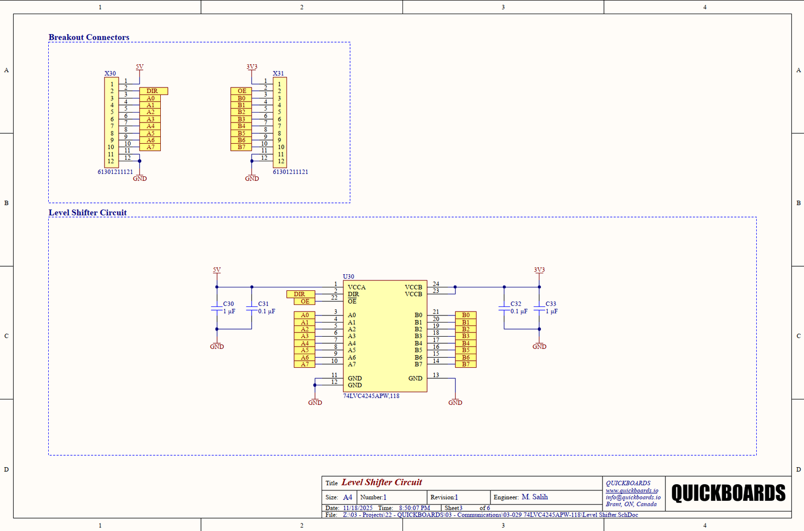
This schematic block features the 74LVC4245APW‑118, an octal dual‑supply bidirectional voltage‑level translating transceiver. It’s designed to bridge between buses operating at different logic‑levels, making it ideal for systems with mixed 3 V and 5 V domains.
Packaged in a 24‑pin TSSOP (thin shrink small‑outline) format, this breakout‑style module provides access to eight bidirectional channels, a direction control pin (DIR), and an output‑enable pin (OE) for bus isolation. The device supports isolating the A‑ and B‑side buses when required, and features high‑impedance outputs when disabled, enabling safe interfacing across voltage domains.
Key Features:
- Eight bidirectional channels in a single‑circuit transceiver
- Dual supply domains: VCCA (1.5 V–5.5 V) and VCCB (1.5 V–3.6 V)
- 5 V‑tolerant inputs/outputs suitable for 5 V logic interfacing
- Output enable (OE) input drives all channels into high‑impedance state when active
- Direction control (DIR) input selects data flow direction A → B or B → A
- Very low standby current / CMOS low‑power consumption
- Operating ambient range: –40 °C to +125 °C typical specification
- TSSOP‑24 surface‑mount package, ideal for high‑density designs
Typical Applications:
- Logic‑level translation between 3.3 V and 5 V microcontrollers or sensors
- Mixed‑voltage bus systems in embedded boards
- Interfacing legacy 5 V logic to modern 3 V logic domains
- System board design requiring bidirectional data buses (e.g., I²C/SMBus, GPIO expansion)
- Reference breakout for multi‑channel signal isolation and buffering
By integrating this Quickboards schematic block, engineers can rapidly create a reliable reference design for voltage‑domain crossing, reduce board complexity by using a single 8‑channel translator instead of multiple discrete devices, and leverage a proven architecture for robust multi‑voltage interconnects.
| Primary IC | 74LVC4245APW-118 |
|---|---|
| IC Datasheet | https://assets.nexperia.com/documents/data-sheet/74LVC4245A.pdf |
| Associated Hardware | HB030292024 |